Comparing tunneling spectroscopy and charge sensing of
Andreev bound states in a semiconductor-superconductor hybrid nanowire structure
Abstract
Transport studies of Andreev bound states (ABSs) are complicated by the interplay of charging effects and superconductivity. Here, we compare transport approaches to ABS spectroscopy in a semiconductor-superconductor island to a charge-sensing approach based on an integrated radio-frequency single-electron transistor. Consistency of the methods demonstrates that fast, non-invasive charge sensing allows accurate quantitative measurement of ABSs while eluding some complexities of transport.
Experiments with superconductor-semiconductor hybrid structures have demonstrated the presence of Andreev bound states (ABSs) in proximitized semiconductors by a variety of methods, including tunneling spectroscopy in NIS junctions (N is normal, S is superconductor, I is an insulating tunnel barrier), Coulomb blockade spectroscopy in superconducting islands with normal leads (NISIN) Higginbotham et al. (2015); Albrecht et al. (2016); Shen et al. (2018); Deng et al. (2016); Vaitiekėnas et al. (2020), and SNS spectroscopy of Josephson junctions Laroche et al. (2019); van Zanten et al. (2020); Sabonis et al. (2020); Kringhøj et al. (2021); Tosi et al. (2019); Hays et al. (2020, 2018); van Woerkom et al. (2017). These methods reveal distinct spectroscopic features and raise different technical challenges. With growing interest in detecting and controlling Majorana zero modes (MZMs) across Josephson junctions Ginossar and Grosfeld (2014); Hassler et al. (2011); Hyart et al. (2013) and distinguishing them from ABSs, it is important to compare methods in systems that can be probed several ways.
In this Article, we report measurements of an electrostatically gated multi-segment hybrid InAs/Al nanowire (NW) device [see Fig. 1(a)] that is reconfigurable in situ, allowing a comparison of spectroscopic signatures of the same ABS by three methods: a Josephson junction (SIS), a Coulomb island (SISIN), and a radio-frequency (RF) charge sensor. We observed consistency between methods, noting that RF charge detection was especially fast, and, unlike transport, does not alter charge occupancy during measurement.
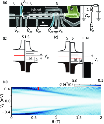
The device was fabricated from an InAs NW grown by molecular beam epitaxy, with Al grown on three facets of the hexagonal core. Using conventional lithographic processing, Al was removed by wet etching in 100 nm segments adjacent to cutter gates C1 and C2, providing gate-controllable barriers. Blanket atomic layer deposited insulated all gates from the NW. Depleting the InAs with C1 and C2 yielded an SISIN device with an S island separated by tunnel barriers (I) from an S lead on the left and N lead on the right. Voltages applied to plunger gates P1-P3 tuned carrier density in adjacent proximitized semiconductor regions as well as the charge offset on the S island. At the far right, a bare InAs segment (again, created by etching of Al), served as RF single-electron transistor (RF-SET) that was capacitively coupled to the main S island by a floating gate [see Fig. 1(a)]. Data acquisition followed Ref. van Zanten et al. (2020) and charge sensing followed Ref. Razmadze et al. (2019). Measurements were performed in a dilution refrigerator with a 6-1-1 T vector magnet.
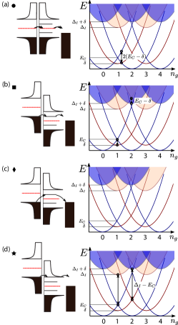
To generate ABSs in the nanowire, we applied a moderate magnetic field, = 600 mT, along the nanowire axis and set gate C1 to the tunneling regime (conductance ), junction C2 to the open regime (), and gates P1-P3 to V to reduce density in the NW. In this configuration, SIS spectroscopy [Figs. 1b)] was used to locate a single subgap state by tuning P3. Figure 1(d) shows differential conductance as a function of bias and in this SIS configuration. Near a precursor of the finite-field ABS is seen at V. Increasing leads to a single ABS moving down with an effective factor of . Starting at T [red marker in Fig. 1(d)] the feature at = 220 V becomes independent of the further increase . This presumably results from competition between a reduction of the induced superconducting gap and a zero-energy-crossing ABS Shen et al. (2018). Unless otherwise noted, measurements described below are at = 0.6 T.
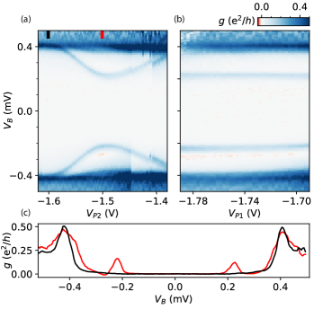
The location of the ABS within the NW could be inferred from its dependence on P1 and P2. Specifically, spectroscopy showed little response to and a strong response to , as shown in Figs. 2(a,b), indicating that the ABS was located on the right side of cutter gate C1, as represented in Fig. 1(b). The energy of the ABS approached the gap edge for V and V with a minimum at around V. Differential conductance as a function of bias, , and gate P1 [Fig. 2(c)] were carried out at V.
Following SIS spectroscopy, gates C1 and C2 were set to the tunneling regime to create a superconducting island, providing SISIN spectroscopy. Figure 3(a) shows the resulting two-dimensional conductance map as a function of bias and island plunger voltage . In the SISIN configuration, transport showed 1-periodic resonances at high bias, V, and 2-periodic features at low bias. The black dashed diagonal line in Fig. 3(a) indicates the alignment of the chemical potential of the left lead and the island. Four features along this diagonal are highlighted: Near , faint 2-periodic features that become stronger along the diagonal at V (), accompanied by negative differential conductance (NDC); Further increasing bias yielded stronger 1-periodic features starting at V () along with stronger NDC; Around V () the conductance increase was largely independent of ; Finally, at V the strong 1-periodic conductance resonances () were observed.
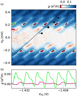
These marked features in Fig. 3(a) are consistent with a model of an SISIN device with a single ABS at energy on the S island with electrostatic energy , where is the charging energy, is the number of electrons on the island, and is the dimensionless gate voltage. In particular, the 2-periodic features at zero bias arise from resonant Cooper pair tunneling between S lead and S island at odd integer values of . At increased bias, the resonance occurs at [dashed line in Fig. 3(a)], with the S island on resonance with the left S lead while the energy difference from the Fermi level in the N lead increases. For the case , the 2-periodic features are expected to be suppressed around zero bias, as Cooper pair resonances are between excited states above the odd parity ground state of the occupied ABS close to odd integer values of . The 2-periodic features around zero bias in Fig. 3(a) suggest that indeed . At [ in Fig. 3(a)], the ABS can empty into the right normal lead, enabling resonant Cooper pair tunneling, brightening the 2-periodic feature. At yet larger bias with fixed , the resonance condition for Cooper pair tunneling from left is exceeded, resulting in NDC. At [ in Fig. 3(a)] above-gap quasiparticles in the left S lead can excite the ABS thus allowing single-electron transport that no longer requires resonant Cooper pair processes, resulting in 1-periodic resonances in . Here, NDC presumably results when the coherence peak in the density of states the S lead surpasses the bound state energy. At [ in Fig. 3(a)] quasiparticles from the S lead can transfer to the N lead via elastic cotunneling through the ABS or other subgap states, which are only weakly dependent on . Finally, at [ in Fig. 3(a)] single-electron transport between continuum states of the left S lead and the S island become energetically allowed. Figure 3(b) shows line cuts from Fig. 3(a), indicating both 2 (pink) and 1 (green) features along with the associated NDC. Further details of the four features are discussed in Appendix .2.
We extract a charging energy 85 eV from independent transport data of Coulomb diamonds (not shown). Using this value, the above model is consistent with an ABS energy eV and superconducting gaps eV and eV, in the left S lead and S island, both consistent with values seen in similar hybrid nanowires Chang et al. (2015). The condition is consistent with the 2 features at low bias in Fig. 3(a).
Transport features observed in SISIN spectroscopy are rather complicated, even with the relatively simple situation of a single ABS on the island. Previous work has showed that RF charge readout offers some advantages compared to transport, particularly speed and simplicity of the data Razmadze et al. (2019); van Veen et al. (2019); de Jong et al. (2019). To perform charge readout on the present device, we use the integrated charge sensor and examine the same ABS investigated above via transport.
Figure 4(a) shows transport-based Coulomb blockade spectroscopy in the SISIN configuration performed over a larger range of P2 gate voltages. The effect of the ABS can be seen as an envelope modulation of Coulomb blockade that follows the shape of the ABS that was previously shown in the Fig. 2(a). To emphasize that the modulation is connected to the ABS, red markers in Fig. 4(a) indicate the tips of Coulomb diamonds. Charge sensing data from the same gate regime as Fig. 4(a) is shown in Fig. 6. Charge sensing shows explicitly the transition in periodicity of superconducting island occupancy whenever the bound state energy is lowered with respect to charging energy of the island. This change in occupancy was implied by the model, but not explicitly visible in transport data. Figure 4(b) shows the effect of the 2 to 1 transition as a function of plunger voltage measured with the the integrated RF-SET. The small overshoot of the even level (blue) at = 1.51 V is associated to ABS that is oscillating around zero energy as a function of . Gate P3 in the Fig. 6 is also responsible for tuning the ABS however with a smaller lever arm compared to P2 compatible with the ABS being localized closer to the barrier C1 side. We note that the suppression of the 2-periodic signal around zero bias in Fig. 4(a) is correlated with the onset of 1-periodicity in Fig. 4(b). This indicates that the exchange of Cooper pairs between the island and superconducting left lead, despite being aligned in chemical potential, is indeed suppressed when . The latter requirement is supported by the observation of re-entrant resonant Cooper pair processes at .
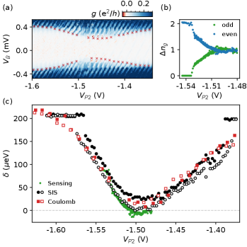
The three measurements methods of the same ABS are compared in Fig. 4(c). Black data points show the ABS profile extracted using SIS spectroscopy [Fig. 2(a)], red - Coulomb blockade measurements where the ABS energy is determined using the onset of Coulomb blockade features [Fig. 4(a)] and green - RF-SET measurements [Fig. 6]. For SIS and SISIN transport measurements both positive and negative values of were used. An offset in of 30 mV between SIS and SISIN measurements, presumably due to cross-capacitance to has been removed. Correspondence between the ABS energy profiles measured using transport (SIS and SISIN) and charge sensing shows that the charge periodicity of the island is indeed affected by the ABS energy. It also shows that RF measurements with increased acquisition rate Razmadze et al. (2019); de Jong et al. (2021) is a useful alternative to transport.
Appendices
.1 Transport processes
Figure 5 shows schematics of the transport processes corresponding to the markers in Fig. 3(a), within our model. In Fig. 5(a) the 2-periodic process at = () is visualized. Typically Cooper pair transfer is resonant around odd integer values. However, in the case of a subgap state energy the 2 transport is blocked. At the transport can get unblocked by emptying the subgap state into the right normal lead. Panel (b) depicts 1-periodic process at bias = ( ) (). The island can relax its energy when going from the even to the odd parity state around odd integer values or from odd parity to even parity at even values. The relaxation reduces the bias threshold for single-electron transfers from the left lead. In Fig. 5(c) a single-electron process at = () can be associated with elastic cotunneling through the bound state or other subgap states. In Fig. 5(d), again, a 1-periodic process at bias = + () happens. This process is similar to (b). The system can save an energy for the threshold when going from even parity state to odd parity state around odd integer or from odd to even parity at even integer values of . Both (b) and (d) require poisoning or some other way of bringing the island out of its ground state. Since both of these are at substantial bias it becomes possible to create the corresponding excited quasiparticle states, for example by splitting a Cooper pair from the left lead (thus gaining energy ) to create two quasiparticles on the island.
.2 Charge sensing of bound state
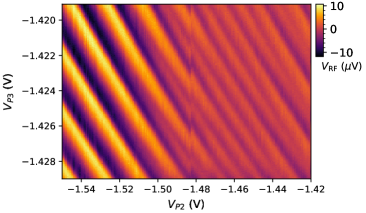
The charge sensor was capacitively coupled to the superconducting island via floating coupler. Fig. 6 shows a two dimensional gate map recorded in demodulated voltage from the charge sensor as a function of gate voltages and (line average along axis subtracted). Measurements are performed at = 0. Constant charge positions appear as bright plateaus interrupted by transitions between the two charge states (dark). The jump at = 1.485 V is likely due to electrostatic background charges in the nanowire environment or in the dielectric covering the nanowire. The effect of the ABS can be seen as a change of gate space periodicity along the axis. It starts from 2-periodic behaviour at more negative values of . Then as the ABS energy is lowered starting at = 1.490 V it transitions through the even-odd and eventually 1 regime recovering back to 2 for more positive values of . Gate P3 is also responsible for tuning the ABS however with a smaller lever arm compared to P2 compatible with the ABS being localised closer to the barrier C1 side.
.3 Fabrication and measurement
The 100 nm diameter nanowire is grown using the vapor-liquid-solid technique in a molecular beam epitaxy system with the InAs [111] substrate crystal orientation. Following the growth, Al is deposited epitaxially in situ on three facets of the nanowire with an average thickness of 10 nm. The nanowire is then positioned by hand on the substrate using a micro-manipulator tool, which gives few-micrometer placement precision. Using standard lithography, the nanowire is patterned and Al is etched away where tunneling barrier controlling gates are defined. Ti/Au contacts and gates are then patterned and thermally evaporated.
Signal demodulation was carried out using a Zurich Instruments Ultra High Frequency Lock-in (ZIUHFLI) access: https://www.zhinst.com/products/uhfli which uses digital processing but the principle of operation is similar to analog demodulation.
Acknowledgments
We thank Shivendra Upadhyay for help with fabrication. Research was supported by Microsoft, the Danish National Research Foundation, and the European Research Council under grant 716655. Judith Suter acknowledges financial support from the Werner Siemens Foundation Switzerland.
References
- Higginbotham et al. (2015) A. P. Higginbotham, S. M. Albrecht, G. Kiršanskas, W. Chang, F. Kuemmeth, P. Krogstrup, T. S. Jespersen, J. Nygård, K. Flensberg, and C. M. Marcus, Nat. Phys. 11, 1017 (2015).
- Albrecht et al. (2016) S. M. Albrecht, A. P. Higginbotham, M. Madsen, F. Kuemmeth, T. S. Jespersen, J. Nygård, P. Krogstrup, and C. M. Marcus, Nature 531, 206 (2016).
- Shen et al. (2018) J. Shen, S. Heedt, F. Borsoi, B. van Heck, S. Gazibegovic, R. L. M. Op het Veld, D. Car, J. A. Logan, M. Pendharkar, S. J. J. Ramakers, G. Wang, D. Xu, D. Bouman, A. Geresdi, C. J. Palmstrøm, E. P. A. M. Bakkers, and L. P. Kouwenhoven, Nat. Commun. 9, 4801 (2018).
- Deng et al. (2016) M. Deng, S. Vaitiekėnas, E. B. Hansen, J. Danon, M. Leijnse, K. Flensberg, J. Nygård, P. Krogstrup, and C. M. Marcus, Science 354, 1557 (2016).
- Vaitiekėnas et al. (2020) S. Vaitiekėnas, G. W. Winkler, B. van Heck, T. Karzig, M.-T. Deng, K. Flensberg, L. I. Glazman, C. Nayak, P. Krogstrup, R. M. Lutchyn, and C. M. Marcus, Science 367 (2020).
- Laroche et al. (2019) D. Laroche, D. Bouman, D. J. van Woerkom, A. Proutski, C. Murthy, D. I. Pikulin, C. Nayak, R. J. J. van Gulik, J. Nygård, P. Krogstrup, L. P. Kouwenhoven, and A. Geresdi, Nat. Commun. 10, 1 (2019).
- van Zanten et al. (2020) D. M. T. van Zanten, D. Sabonis, J. Suter, J. I. Väyrynen, T. Karzig, D. I. Pikulin, E. C. T. O’Farrell, D. Razmadze, K. D. Petersson, P. Krogstrup, and C. M. Marcus, Nat. Phys. , 663 (2020).
- Sabonis et al. (2020) D. Sabonis, O. Erlandsson, A. Kringhøj, B. van Heck, T. W. Larsen, I. Petkovic, P. Krogstrup, K. D. Petersson, and C. M. Marcus, Phys. Rev. Lett. 125, 156804 (2020).
- Kringhøj et al. (2021) A. Kringhøj, G. Winkler, T. Larsen, D. Sabonis, O. Erlandsson, P. Krogstrup, B. van Heck, K. Petersson, and C. M. Marcus, Phys. Rev. Lett. 126, 047701 (2021).
- Tosi et al. (2019) L. Tosi, C. Metzger, M. Goffman, C. Urbina, H. Pothier, S. Park, A. L. Yeyati, J. Nygård, and P. Krogstrup, Phys. Rev. X 9, 011010 (2019).
- Hays et al. (2020) M. Hays, V. Fatemi, K. Serniak, D. Bouman, S. Diamond, G. de Lange, P. Krogstrup, J. Nygård, A. Geresdi, and M. Devoret, Nat. Phys. , 1103 (2020).
- Hays et al. (2018) M. Hays, G. De Lange, K. Serniak, D. van Woerkom, D. Bouman, P. Krogstrup, J. Nygård, A. Geresdi, and M. Devoret, Phys. Rev. Lett. 121, 047001 (2018).
- van Woerkom et al. (2017) D. J. van Woerkom, A. Proutski, B. van Heck, D. Bouman, J. I. Väyrynen, L. I. Glazman, P. Krogstrup, J. Nygård, L. P. Kouwenhoven, and A. Geresdi, Nat. Phys. 13, 876 (2017).
- Ginossar and Grosfeld (2014) E. Ginossar and E. Grosfeld, Nat. Commun. 5, 1 (2014).
- Hassler et al. (2011) F. Hassler, A. Akhmerov, and C. Beenakker, New J. of Phys. 13, 095004 (2011).
- Hyart et al. (2013) T. Hyart, B. van Heck, I. Fulga, M. Burrello, A. Akhmerov, and C. Beenakker, Phys. Rev. B 88, 035121 (2013).
- Razmadze et al. (2019) D. Razmadze, D. Sabonis, F. K. Malinowski, G. C. Ménard, S. Pauka, H. Nguyen, D. M. van Zanten, E. C. O′Farrell, J. Suter, P. Krogstrup, F. Kuemmeth, and C. M. Marcus, Phys. Rev. Appl. 11, 064011 (2019).
- Chang et al. (2015) W. Chang, S. Albrecht, T. Jespersen, F. Kuemmeth, P. Krogstrup, J. Nygård, and C. M. Marcus, Nat. Nanotechnol. 10, 232 (2015).
- van Veen et al. (2019) J. van Veen, D. de Jong, L. Han, C. Prosko, P. Krogstrup, J. D. Watson, L. P. Kouwenhoven, and W. Pfaff, Phys. Rev. B 100, 174508 (2019).
- de Jong et al. (2019) D. de Jong, J. van Veen, L. Binci, A. Singh, P. Krogstrup, L. P. Kouwenhoven, W. Pfaff, and J. D. Watson, Phys. Rev. Appl. 11, 044061 (2019).
- de Jong et al. (2021) D. de Jong, C. Prosko, D. Waardenburg, L. Han, F. K. Malinowski, P. Krogstrup, L. P. Kouwenhoven, J. V. Koski, and W. Pfaff, arXiv preprint arXiv:2103.03659 (2021).
- (22) E. access: https://www.zhinst.com/products/uhfli, .