Charge density waves and Fermi level pinning in monolayer and bilayer SnSe2
Abstract
Materials with reduced dimensionality often exhibit exceptional properties that are different from their bulk counterparts. Here we report the emergence of a commensurate 2 2 charge density wave (CDW) in monolayer and bilayer SnSe2 films by scanning tunneling microscope. The visualized spatial modulation of CDW phase becomes prominent near the Fermi level, which is pinned inside the semiconductor band gap of SnSe2. We show that both CDW and Fermi level pinning are intimately correlated with band bending and virtual induced gap states at the semiconductor heterointerface. Through interface engineering, the electron-density-dependent phase diagram is established in SnSe2. Fermi surface nesting between symmetry inequivalent electron pockets is revealed to drive the CDW formation and to provide an alternative CDW mechanism that might work in other compounds.
Charge density wave (CDW) represents a static modulation of conduction electrons that is commonly accompanied by a periodic lattice distortion Monceau (2012). The understanding of such a collectively ordered electronic state has been widely supposed to be a key to decipher the secrets of unconventional superconductivity in many two-dimensional (2D) layered materials due to their close proximity in the electronic phase diagram Keimer et al. (2015); Isobe et al. (2018). In quest of this objective, dimensionality and interface engineering have been often considered as unique strategies to create and control the CDW phase Calandra et al. (2009); Soumyanarayanan et al. (2013); Lin et al. (2020); Frano et al. (2016). As a matter of fact, newly emerging or enhanced CDW correlations have been revealed in several transition metal dichalcogenides at the 2D limit Peng et al. (2015); Xi et al. (2015); Chen et al. (2017); Duvjir et al. (2018), whereas the interfacial effects on the CDW order of these 2D nanosheets were relatively little investigated Lefcochilos-Fogelquist et al. (2019); Jia et al. (2018). A variety of scenarios invoking the saddle-point singularities Rice and Scott (1975), Fermi surface nesting Monceau (2012); Duvjir et al. (2018), electron-phonon coupling Xi et al. (2015), excitonic insulator Wilson (1977); Kogar et al. (2017) and Jahn-Teller band instabilities Chen et al. (2017); Whangbo and Canadell (1992), as well as some combination of them Kidd et al. (2002), have been employed to account for the formation of CDW. However, a consensus on which factors play the primary roles in driving the CDW transition remains a hotly debated topic.
On the other hand, layered main-group metal dichalcogenides like SnSe2 have recently attracted substantial interest owing to their potential applications in field-effect transistors Guo et al. (2016), optoelectronic Zhou et al. (2015); Huang et al. (2015) and thermoelectric devices Luo et al. (2018), while the high abundance and low toxicity of Sn hold promises for the commercial use. Interface engineering via organometallic intercalation Wu et al. (2019); Song et al. (2019), heterostructure design Zhang et al. (2018a); Shao et al. (2019) and dielectric gating techniques Zeng et al. (2018) has led to the emergence of superconductivity in SnSe2, although its bulk counterpart is well-known as semiconductor with an indirect band gap of 1.07 eV Gonzalez and Oleynik (2016). Moreover, periodic lattice distortions, possibly associated with CDW, were ever reported in pressurized and compressed SnSe2 Shao et al. (2019); Ying et al. (2018). Astonishingly, the so-called CDW orders exhibit different wave vectors, calling for further study. Layered 1T-SnSe2 has thus become a newly-fertile playground for the exploration and manipulation of these many-body collective phenomena, as well as the interplay between them. In this study, we employ scanning tunneling microscopy (STM) to exploit interface-induced CDW order and Fermi level () pinning in monolayer (ML) and bilayer (BL) SnSe2 films prepared on Sn-terminated Si(111) and SrTiO3(001) substrates. Virtual induced gap states (VIGSs) at the semiconductor heterointerface are visualized and found to correlate intimately with the occurrence of CDW and pinning in ultrathin SnSe2.
All experiments were carried out in an ultrahigh vacuum cryogenic STM system (Unisoku), which is connected to a molecular beam epitaxy (MBE) for in-situ sample preparation. The base pressure of both chambers is better than 1.0 10-10 Torr. Arsenic-doped Si(111) wafers were cleaned by repeated flashing to 1200∘C, leading to a reconstructed Si(111)-7 surface, while niobium-doped SrTiO3(001) substrates were heated at 1200∘C for 20 min to get a clean surface. High purity Sn (99.9999) and Se (99.999) sources are co-evaporated from standard effusion cells onto the substrates at 210∘C Zhang et al. (2018a). Due to the very volatile nature of Se molecules from the effusion cell, a high Se/Sn flux ratio of 10 was used to compensate for the Se losses during the MBE growth, bearing a similar growth dynamic to that for other metal selenides Song et al. (2011). After the film growth, the samples were immediately transferred into the STM stage for data collection at 4.5 K, unless otherwise specified. Polycrystalline PtIr tips were conditioned by electron beam heating, calibrated on Ag/Si(111) films and used throughout the experiment. Tunneling conductance spectra were measured by using a standard lock-in technique with a small bias modulation at 931 Hz.
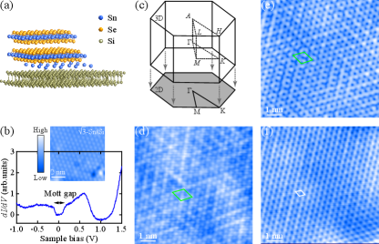
Layered 1T-SnSe2 has a trigonal symmetry and consists of hexagonally packed Sn sheets sandwiched between the anionic Se sheets with an in-plane lattice parameter of approximately 3.81 Å Gonzalez and Oleynik (2016). In order to optimize the epitaxial growth of SnSe2 thin films, freshly cut Si(111) substrates with an in-plane lattice parameter of 3.8403 Å are ideally chosen [Fig. 1(a)], yielding a lattice mismatch of . We further passivate the chemically reactive Si(111)-7 substrates by depositing 1/3 ML Sn atoms at 600∘C, as detailed in the Supplemental Materials sup . This results into a Sn-terminated Sn/Si(111)- (hereafter referred to as -Sn/Si) surface, characteristic of a Mott-Hubbard insulating ground state [Figs. 1(b) and S1] Modesti et al. (2007); Wu et al. (2020). Figure 1(c) depicts the three-dimensional (3D) Brillouin zone of SnSe2 with high symmetry points and its 2D projection. Recent first-principles calculations and band structure measurements of SnSe2 have located its conduction band minimum (CBM) and valence band maximum (VBM) along the - and -() directions Gonzalez and Oleynik (2016); Lochocki et al. (2019), respectively. This differs from the CDW-bearing sister compound 1T-TiSe2 with the VBM located justly at Jia et al. (2018). Besides, TiSe2 has been widely considered to be a semimetal or a narrow-gap semiconductor Wilson (1977); Kidd et al. (2002); Lochocki et al. (2019), whereas the semiconducting SnSe2 exhibits a gap greater than 1.0 eV Gonzalez and Oleynik (2016). Despite these distinctions, ML and BL SnSe2 films grown on -Sn/Si exhibit a clear charge order [Figs. 1(d) and 1(e)]. In analogy to 1T-TiSe2, the CDW modulation displays a commensurate 2 2 structure. More remarkably, the CDW vanishes in triple-layer (TL) SnSe2, leaving behind an intact SnSe2(001)-1 1 surface [Fig. 1(f)].
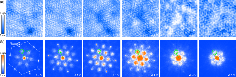
Provided that the lattice mismatch between SnSe2 and the Si(111) substrate is negligibly small, we exclude that the observed CDW phase origins from any possible effects associated with the epitaxial strain Shao et al. (2019). To understand the microscopic cause of the CDW order, we show a series of bias-dependent STM topographies and the corresponding fast Fourier transform (FFT) images in Figs. 2 and S2. Evidently, the CDW spots, marked by the green circles, become more prominent near . This is understandable since a CDW phase transition mainly affects the density of states (DOS) of SnSe2 close to . More interestingly, the CDW wave vector reduces below 0.1 eV [Fig. S3], leading to a crossover from commensurate to incommensurate CDW state.
Figure 3(a) plots the CDW intensity (top panel), calculated as integrated FFT magnitude from the green circled regions in Fig. 2(b), as a function of the bias. As expected, the CDW is suppressed at an elevated temperature of 78 K. Compared to BL SnSe2, ML SnSe2 displays more pronounced CDW. This hints at the essential importance of interfacial effects in the CDW formation. A careful investigation of SnSe2 thickness-dependent dI/dV spectra in the bottom panel of Fig. 3(a) reveals an enhancement of the direct band gap E() upon reduction of the film thickness. This is consistent with a previous report Zhang et al. (2018a) and could be accounted for in terms of the poor electrostatic screening and enhanced quantum confinement in few-layer SnSe2 Gonzalez and Oleynik (2016). More significantly, we find that on the surface is pinned 0.40.5 eV below the CBM at , irrespective of the SnSe2 film thickness.
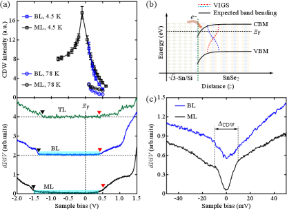
The formation of CDW phase and pinning in ultrathin SnSe2 films are closely related to emergent electronic states in the semiconducting gap, i.e. the cyan-marked finite DOS in Fig. 3(a). The in-gap states get suppressed with thickness and could not be ascribed to any impurity-induced bound states, because there exists little defect on the SnSe2 films investigated [Figs. 1(d)-(f)]. Knowing that SnSe2 has a large electron affinity Zhang et al. (2018b), upon contact electrons would flow from -Sn/Si to SnSe2, leading to downward band bending of the SnSe2 and confinement of 2D electron gas (2DEG) at the interface [Fig. 3(b)]. This might contribute to some in-gap states predominantly near the CBM at the M points of the 2D Brillouin zone. More significantly, VIGSs will develop at the SnSe2/-Sn/Si semiconductor heterointerface and extend over the whole indirect band gap of SnSe2 Lüth (2001). The VIGSs correspond to the imaginary components of the complex wave function and exponentially decay away from the interface Lüth (2001). As predicted, the decay lengths critically rely on the energy and diverge at the conduction and valance band edges for the VIGSs with conduction-band character and valance-band character, respectively. As a consequence, more conduction (valance)-derived VIGSs emerge around CBM and VBM, marked by the red (blue) dashed lines in Fig. 3(b). Based on the one-dimensional VIGS model Monch (1990), the minimum decay length of VIGSs occurs roughly at the midgap energy and approximates to 6.0 Å for SnSe2. This is consistent with the sharply suppressed in-gap states on BL and TL SnSe2 (see the bottom panel of Fig. 3(a)). Plotted in Fig. 3(c) are the smaller-energy-scale tunneling spectra of ML and BL SnSe2 films. Partial gaps associated with the CDW phase are identified in the vicinity of . The gap magnitude 20 meV agrees quantitatively with the significant suppression of CDW at 78 K [Fig. 3(a)].
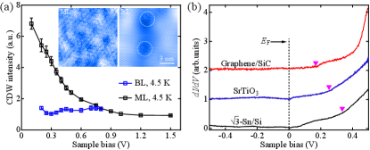
In order to provide more insights into the CDW phase of SnSe2, we also prepare ultrathin SnSe2 films on SrTiO3 substrate. Distinct from a recent report Shao et al. (2019), no apparent lattice compression is revealed. This seems more understandable because the MBE growth of layered SnSe2 films is of quasi-van der Waals epitaxy. Shown in Fig. 4(a) are STM topographies and energy dependent CDW intensity in ML and BL SnSe2/SrTiO3 films. Evidently, the CDW modulations are weaker than those in SnSe2/-Sn/Si. In particular, only short-ranged CDW order, circled by the white dashes in Fig. 4(a), could be seen to surround single native defects in BL SnSe2/SrTiO3 films.
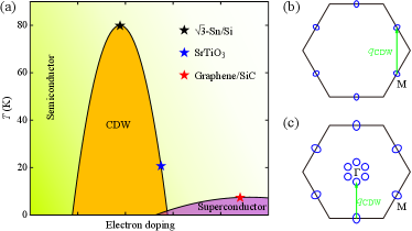
Figure 4(b) compares the tunneling dI/dV spectra of monolayer SnSe2 films on the indicated substrates, with the MBE growth of SnSe2 on graphene/SiC substrate described in detail elsewhere Zhang et al. (2018a). The conductance kinks, marked by magenta triangles, correspond to the CBM at M. The emergence of VIGSs proves generic for all three heterostructures and serve as a reservoir for electrons/holes. These states effectively pin and hold the key for the CDW formation in ML and BL SnSe2. Given that the band bending and VIGS decay length are determined primarily by the semiconductor parameters of SnSe2 Monch (1990); Kerelsky et al. (2017), the smaller energy spacing between the CBM at the M points and means more electron doping. Such distinction may be probably related to the different work function of the substrates. Anyhow, our comparison study enables to establish a doping-dependent phase diagram of SnSe2 in Fig. 5(a). Upon electron doping via interface engineering, the CDW develops with the filled VIGSs in ML and BL SnSe2/-Sn/Si films. As the electron doping is further increased, the CDW phase gets suppressed in ultrathin SnSe2/SrTiO3 films and eventually evolves into a superconducting state when the SnSe2 films are grown on a graphitized SiC(0001) substrate Zhang et al. (2018a). This complete electronic phase diagram highlights the importance of dimensionality and electron doping in SnSe2 semiconductor, and offers fresh insights into the relationship between the CDW phase and superconductivity.
We now discuss possible mechanisms for the observed CDW phase. The large semiconductor band gap of 1.07 eV prevents an excitonic insulator scenario from being responsible for the CDW order in SnSe2, where an exciton binding energy larger than the band gap is needed but hardly fulfilled Wilson (1977). This holds even more true for ultrathin SnSe2 films with enhanced band gap [Fig. 3(a)]. Secondly, a Jahn-Teller band instability, as widely explored for explaining CDW in Ti-based dichalcogenides Chen et al. (2017); Rossnagel et al. (2002); Rossnagel (2010), could be safely excluded as well. This is primarily because a starting point of the band-type Jahn-Teller interaction is the substantial overlap of conduction and valance bands, which is yet separated by the semiconductor band gap in SnSe2. Moreover, this model relates intimately to a low-lying d-orbital splitting Hughes (1977) or a s-d orbital mixing Whangbo and Canadell (1992). Distinct from TiSe2, however, the d orbital is little involved in the conduction and valance bands of the s-p metal dichalcogenide SnSe2 Gonzalez and Oleynik (2016). As thus, our results call for other scenarios for the formation of CDW in SnSe2. Obviously, any models associated with saddle-point singularities are unlikely, since of the SnSe2 films is well pinned inside the band gap and no sharp DOS enhancement is observable around [Figs. 3(a) and 4(b)].
Next we resort to a classical concept of CDW order induced by Fermi surface nesting Monceau (2012). This is in agreement with our observation of CDW only in the presence of sufficient in-gap states or electronic DOS around . Multilayered and bulk SnSe2 without low-lying DOS exhibit no CDW. Since of ultrathin SnSe2 films lies closer to the CBM(M) than VBM(), the electronic DOS in the vicinity of originates predominantly from the band bending confined 2DES and VIGSs with conduction-band character at M, illustrated in Fig. 5(b). There exists little DOS at , and thus a simple Fermi surface nesting connecting the CBM(M) than VBM() seems unlikely. Alternatively, the Fermi surface nesting between symmetry inequivalent electron pockets at M, marked by the green arrow in Fig. 5(b), might be the driving force for the CDW formation. This is especially true as the electron pockets are small and the Fermi surface can nest nicely at the wave vector of the commensurate 2 2 CDW order observed. Here the elastic energy cost of lattice modulation is compensated by the total electronic energy gain via opening a gap at [Fig. 3(c)] and pushing the nearby states to lower energies. Upon additional electron doping, the electron pockets become larger, deteriorating the Fermi surface nesting for the CDW phase. As the CDW phase is almost killed due to the poor Fermi surface nesting, the superconductivity occurs probably associated with the intrapocket scattering at M. They seem fitting neatly to the electronic phase diagram in Fig. 5(a).
Finally, we note that as the applied bias is lowered far below , i.e. roughly at the midgap energy of 0.7 eV [Fig. 2], VIGSs with the valance-band character develop equivalently near , prompting substantial scattering between the - and M-near VIGSs [Fig. 5(c)] at the given energy. Provided that the VBM and thus the valance-band-derived DOS are not strictly located at Gonzalez and Oleynik (2016); Lochocki et al. (2019), the scattering wave vector should be smaller than that of 2 2 order. This will induce a commensurate-to-incommensurate transition of the CDW order, as observed above. The incommensurate CDW is found to run along the -M direction [Fig. 2]. This indicates that the VBM orient along the -M direction as well Gonzalez and Oleynik (2016), rather than the -K direction.
Our detailed STM study has revealed a commensurate 2 2 CDW phase in ultrathin SnSe2 epitaxial films prepared on both -Sn/Si and SrTiO3 substrates. Such a collectively ordered state is found to correlate intimately with the band bending and emergent VIGSs at the semiconductor heterointerfaces. We propose a novel mechanism associated with Fermi surface nesting between the symmetry inequivalent electron pockets at M to account for the formation of CDW nicely. The present method of interface engineering opens up possibilities in searching for novel states of matter at the 2D limit.
Acknowledgements.
This work is financially supported by the National Natural Science Foundation of China (Grants No. 11774192, No. 11634007), the Ministry of Science and Technology of China (Grants No. 2016YFA0301004, No. 2017YFA0304600, No. 2018YFA0305603), and in part by the Beijing Advanced Innovation Center for Future Chip.References
- Monceau (2012) P. Monceau, Adv. Phys. 61, 325 (2012).
- Keimer et al. (2015) B. Keimer, S. Kivelson, M. Norman, S. Uchida, and J. Zaanen, Nature 518, 179 (2015).
- Isobe et al. (2018) H. Isobe, N. F. Q. Yuan, and L. Fu, Phys. Rev. X 8, 041041 (2018).
- Calandra et al. (2009) M. Calandra, I. I. Mazin, and F. Mauri, Phys. Rev. B 80, 241108 (2009).
- Soumyanarayanan et al. (2013) A. Soumyanarayanan, M. M. Yee, Y. He, J. Van Wezel, D. J. Rahn, K. Rossnagel, E. W. Hudson, M. R. Norman, and J. E. Hoffman, Proc. Natl. Acad. Sci. USA 110, 1623 (2013).
- Lin et al. (2020) D. J. Lin, S. C. Li, J. S. Wen, H. Berger, L. Forró, H. B. Zhou, S. Jia, T. Taniguchi, K. Watanabe, X. X. Xi, and M. S. Bahramy, Nat. Commun. 11, 1 (2020).
- Frano et al. (2016) A. Frano, S. Blanco-Canosa, E. Schierle, Y. Lu, M. Wu, M. Bluschke, M. Minola, G. Christiani, H. U. Habermeier, G. Logvenov, Y. Wang, P. A. van Aken, E. Benckiser, E. Weschke, M. L. Tacon, and B. Keimer, Nat. Mater. 15, 831 (2016).
- Peng et al. (2015) J. P. Peng, J. Q. Guan, H. M. Zhang, C. L. Song, L. Wang, K. He, Q. K. Xue, and X. C. Ma, Phys. Rev. B 91, 121113 (2015).
- Xi et al. (2015) X. X. Xi, L. Zhao, Z. F. Wang, H. Berger, L. Forró, J. Shan, and K. F. Mak, Nat. Nanotechnol. 10, 765 (2015).
- Chen et al. (2017) P. Chen, W. W. Pai, Y. H. Chan, A. Takayama, C. Z. Xu, A. Karn, S. Hasegawa, M. Y. Chou, S. K. Mo, A. V. Fedorov, and T. C. Chiang, Nat. Commun. 8, 1 (2017).
- Duvjir et al. (2018) G. Duvjir, B. K. Choi, I. Jang, S. Ulstrup, S. Kang, T. Thi Ly, S. Kim, Y. H. Choi, C. Jozwiak, A. Bostwick, E. Rotenberg, J. G. Park, R. Sankar, K. S. Kim, J. Kim, and Y. J. Chang, Nano Lett. 18, 5432 (2018).
- Lefcochilos-Fogelquist et al. (2019) H. M. Lefcochilos-Fogelquist, O. R. Albertini, and A. Y. Liu, Phys. Rev. B 99, 174113 (2019).
- Jia et al. (2018) T. Jia, S. N. Rebec, S. Tang, K. Xu, H. M. Sohail, M. Hashimoto, D. Lu, R. G. Moore, and Z. X. Shen, 2D Materials 6, 011008 (2018).
- Rice and Scott (1975) T. M. Rice and G. K. Scott, Phys. Rev. Lett. 35, 120 (1975).
- Wilson (1977) J. A. Wilson, Solid State Commun. 22, 551 (1977).
- Kogar et al. (2017) A. Kogar, M. S. Rak, S. Vig, A. A. Husain, F. Flicker, Y. I. Joe, L. Venema, G. J. MacDougall, T. C. Chiang, E. Fradkin, J. van Wezel, and P. Abbamonte, Science 358, 1314 (2017).
- Whangbo and Canadell (1992) M. H. Whangbo and E. Canadell, J. Am. Chem. Soc. 114, 9587 (1992).
- Kidd et al. (2002) T. E. Kidd, T. Miller, M. Y. Chou, and T. C. Chiang, Phys. Rev. Lett. 88, 226402 (2002).
- Guo et al. (2016) C. Guo, Z. Tian, Y. Xiao, Q. Mi, and J. Xue, Appl. Phys. Lett. 109, 203104 (2016).
- Zhou et al. (2015) X. Zhou, L. Gan, W. Tian, Q. Zhang, S. Jin, H. Li, Y. Bando, D. Golberg, and T. Zhai, Adv. Mater. 27, 8035 (2015).
- Huang et al. (2015) Y. Huang, K. Xu, Z. Wang, T. A. Shifa, Q. Wang, F. Wang, C. Jiang, and J. He, Nanoscale 7, 17375 (2015).
- Luo et al. (2018) Y. B. Luo, Y. Zheng, Z. Z. Luo, S. Q. Hao, C. F. Du, Q. H. Liang, Z. Li, K. A. Khor, K. Hippalgaonkar, J. W. Xu, Q. Y. Yan, C. Wolverton, and M. G. Kanatzidis, Adv. Energy Mater. 8, 1702167 (2018).
- Wu et al. (2019) H. Wu, S. Li, M. Susner, S. Kwon, M. Kim, T. Haugan, and B. Lv, 2D Mater. 6, 045048 (2019).
- Song et al. (2019) Y. P. Song, X. W. Liang, J. G. Guo, J. Deng, G. Y. Gao, and X. L. Chen, Phys. Rev. Materials 3, 054804 (2019).
- Zhang et al. (2018a) Y. M. Zhang, J. Q. Fan, W. L. Wang, D. Zhang, L. Wang, W. Li, K. He, C. L. Song, X. C. Ma, and Q. K. Xue, Phys. Rev. B 98, 220508 (2018a).
- Shao et al. (2019) Z. B. Shao, Z. G. Fu, S. J. Li, Y. Cao, Q. Bian, H. Sun, Z. Y. Zhang, H. Gedeon, X. Zhang, L. L. J. Liu, Z. W. Cheng, F. W. Zheng, P. Zhang, and M. H. Pan, Nano Lett. 19, 5304 (2019).
- Zeng et al. (2018) J. W. Zeng, E. F. Liu, Y. J. Fu, Z. Y. Chen, C. Pan, C. Y. Wang, M. Wang, Y. J. Wang, K. Xu, S. H. Cai, X. X. Yan, Y. Wang, X. W. Liu, P. Wang, S. J. Liang, Y. Cui, H. Y. Hwang, H. T. Yuan, and F. Miao, Nano Lett. 18, 1410 (2018).
- Gonzalez and Oleynik (2016) J. M. Gonzalez and I. I. Oleynik, Phys. Rev. B 94, 125443 (2016).
- Ying et al. (2018) J. J. Ying, H. Paudyal, C. Heil, X.-J. Chen, V. V. Struzhkin, and E. R. Margine, Phys. Rev. Lett. 121, 027003 (2018).
- Song et al. (2011) C. L. Song, Y. L. Wang, Y. P. Jiang, Z. Li, L. Wang, K. He, X. Chen, X. C. Ma, and Q. K. Xue, Phys. Rev. B 84, 020503 (2011).
- (31) See Supplemental Material at for details regarding substrates, FFT images and CDW wave vectors. .
- Modesti et al. (2007) S. Modesti, L. Petaccia, G. Ceballos, I. Vobornik, G. Panaccione, G. Rossi, L. Ottaviano, R. Larciprete, S. Lizzit, and A. Goldoni, Phys. Rev. Lett. 98, 126401 (2007).
- Wu et al. (2020) X. F. Wu, F. F. Ming, T. S. Smith, G. Liu, F. Ye, K. Wang, S. Johnston, and H. H. Weitering, Phys. Rev. Lett. 125, 117001 (2020).
- Lochocki et al. (2019) E. B. Lochocki, S. Vishwanath, X. Y. Liu, M. Dobrowolska, J. Furdyna, H. G. Xing, and K. M. Shen, Appl. Phys. Lett. 114, 091602 (2019).
- Zhang et al. (2018b) Q. Zhang, M. Li, E. B. Lochocki, S. Vishwanath, X. Liu, R. Yan, H.-H. Lien, M. Dobrowolska, J. Furdyna, K. M. Shen, G. J. Cheng, A. R. Hight Walker, D. J. Gundlach, H. G. Xing, and N. V. Nghyen, Appl. Phys. Lett. 112, 042108 (2018b).
- Lüth (2001) H. Lüth, Solid surfaces, interfaces and thin films, Vol. 4 (Springer, 2001).
- Monch (1990) W. Monch, Rep. Prog. Phys. 53, 221 (1990).
- Kerelsky et al. (2017) A. Kerelsky, A. Nipane, D. Edelberg, D. Wang, X. Zhou, A. Motmaendadgar, H. Gao, S. Xie, K. Kang, J. Park, J. Teherani, and A. Pasupathy, Nano Lett. 17, 5962 (2017).
- Rossnagel et al. (2002) K. Rossnagel, L. Kipp, and M. Skibowski, Phys. Rev. B 65, 235101 (2002).
- Rossnagel (2010) K. Rossnagel, New J. Phys. 12, 125018 (2010).
- Hughes (1977) H. P. Hughes, J. Phys. C: Solid State Phys. 10, L319 (1977).