CHARACTERIZATION OF DIM LIGHT RESPONSE IN DVS PIXEL: DISCONTINUITY OF EVENT TRIGGERING TIME
Abstract
Dynamic Vision Sensors (DVS) have recently generated great interest because of the advantages of wide dynamic range and low latency compared with conventional frame-based cameras. However, the complicated behaviors in dim light conditions are still not clear, restricting the applications of DVS. In this paper, we analyze the typical DVS circuit, and find that there exists discontinuity of event triggering time. In dim light conditions, the discontinuity becomes prominent. We point out that the discontinuity depends exclusively on the changing speed of light intensity. Experimental results on real event data validate the analysis and the existence of discontinuity that reveals the non-first-order behaviors of DVS in dim light conditions.
Index Terms— Dynamic vision sensor, dim light conditions, event triggering time, discontinuity, non-first-order behaviors
1 Introduction
Dynamic vision sensors (DVS) detect temporal contrast in light intensity, different from conventional cameras sensing light intensity directly [1, 2, 3, 4, 5]. It imitates human retina, a logarithmic and first-order system sensitive to a fixed light contrast but invariant to absolute light intensity [6]. The humanoid behaviors facilitate the high dynamic range (more than 6 decades), low latency, and energy saving [7].
However, the first-order response does not suit for the DVS in dim light conditions, due to the properties of DVS circuit[4]. The imperfect behaviors in dim light conditions have been studied by researchers. To increase the dynamic range, Delbruck and Mead[1] suppress the non-first-order response in the conventional logarithmic light receptor by an adaptive element and cascode feedback loop. This adaptive photoreceptor invented by Delbruck and Mead is the prototype of recent DVS [8, 9, 10, 11]. Lichtsteiner, Posch, and Delbruck [4] point out that the first-order response is contaminated by the photodiode parasitic capacitor and resistance of the feedback metal-oxide-semiconductor field-effect transistor (MOSFET) without further analysis. Hu, Liu and Delbruck [12] design a widely-used DVS simulator, which forms the operation of DVS in dim light conditions as an infinite impulse response (IIR) low pass filter. Graca and Delbruck [13] research on the shot noise of DVS in dim light conditions, showing the paradox between the first- and second-order systems. Lin, Ma, et al. [14] use Brownian motion with drift for simulation, but the simulated behaviors deviate partly from those of real DVS in dim light conditions. The above researches contribute greatly to the developments of DVS, but lack of further analysis of DVS in dim light conditions which are quite common in practical applications.
In this paper, the typical DVS circuit is studied. We find that there exists discontinuity of event triggering time, which is one of the main factors deciding the DVS’s unsatisfied behaviors in dim light conditions. Based on our analysis, the discontinuity extends with slow changing speed of light intensity. Because the dim light conditions generally share small difference of light intensity, the discontinuity will be prominent. By analyzing the properties of DVS circuit, the discontinuity of event triggering time is attributed to the charge and discharge of parasitic capacitor of photodiode. Experimental results on real data of DVS validate the above analysis and will be helpful for further improvements of DVS, such as design of event simulators. For convenience, the meanings of symbols used in this paper are illustrated in Table. 1.
| symbols | meanings |
|---|---|
| feedback MOS | |
| and | cascode MOS amplifier |
| MOS source follower | |
| MOS providing difference of voltage | |
| photodiode | |
| and | capacitors for differential amplifier |
| parasitic capacitor of PD | |
| light intensity | |
| photocurrent across photodiode | |
| voltage of photodiode | |
| gate voltage of fed back by cascode | |
| drain voltage of buffered from | |
| source voltage of | |
| charge of difference in during triggering of events | |
| time delay between consecutive triggering events | |
| changing speed of light intensity |
2 Discontinuity of event triggering time
In this section, the typical DVS circuit is analyzed along with its operation principle. The charge and discharge of parasitic capacitor of photodiode causes a time delay between triggering events, leading to the discontinuity. The non-first-order behavior is aroused by the duration of discontinuity that depends exclusively on the changing speed of light intensity and photocurrent.
2.1 DVS circuit and operation principle
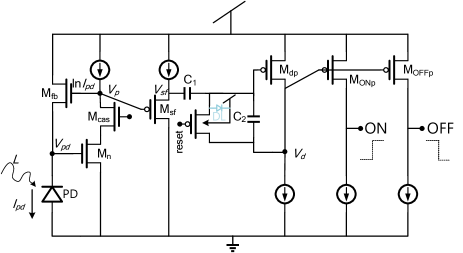
The typical DVS circuit of one pixel is illustrated in . When the light signal on the photodiode is static without change, there will be few events other than some noise induced by the junction leak current of diode DL. Assume that the last event triggers at the time . After time , the incident light on changes from to , and the source voltage of the metal-oxide-semiconductor (MOS) transistor varies from to . In case that the MOS comparators detect that overcomes predefined ON threshold - or OFF threshold , an ON or OFF event is triggered, respectively. The process is formulated as follows:
| (1) |
The source voltage will be reset when the event triggers.
After the introduction of event triggering, we analyze the signal transduction from light signal to electrical signal in the DVS circuit. At time , the photocurrent flowing across the photodiode is . After time , the change of photocurrent is induced in the photodiode that satisfies:
| (2) |
The differential amplifier with capacitors and amplifies that is buffered from and then drives the gate of MOS to control the source voltage [4]:
where is the gain of differential amplifier, and are the slope factors of MOS and , respectively, and is the thermal voltage.
2.2 parasitic capacitor of photodiode
Actually, the photodiode voltage changes with the light signal , despite the clamping by the feedback loop and cascode. The cascode of and senses the change of with amplification. The amplified result is fed back by to accommodate the change of .

In the distributed diagram of photodiode given in , the junction of consists of the parasitic capacitor . As the parallel resistance is extremely high and the series resistance tends to be quite low [15], the charge and discharge of is one of the main reasons for the delay and discontinuity of event triggering time.
Ideally, when there is a light intensity change in time , an immediately stimulated current will flow across . However, in fact this is not the case. In the distributed diagram of photodiode shown in , needs to charge or discharge the parasitic capacitor of , firstly. The process is not completed until the voltage of reaches to accommodate the stimulated current .
2.3 time delay and discontinuity
The charge and discharge of parasitic capacitor is time-consuming, leading to a time delay between triggering events. If we evaluate the triggering time of events, the distribution of triggering time is probably discontinuous because there are few events in the time delay region.
As the photodiode is reverse-biased, the barrier capacitance is dominant in . Compared with the built-in potential of photodiode (usually hundreds of mV) [16], the voltage change of is much smaller (nearly a few mV) [17]. According to [16], the parasitic capacitance of is almost unchanged.
The change of electric charge stored in the capacitor is:
| (4) |
Based on Eqs. 1 and 2.1, the change is fixed between two consecutive events. In the small-signal analysis of cascode,
| (5) |
where is the small-signal gain of cascode.
Therefore, and are invariable between two consecutive triggering events if we do not consider the influence by shot noise, dark current, and leak noise. Assuming that is the fixed electric charge difference, there is a time delay between triggering events:
| (6) |
Note that: 1. is not proportional to (), which means that the time delay follows a non-first-order system rule of DVS; 2. As is only related to the threshold ( and ), is invariant to current light intensity.
In fact, needs some time to change because light intensity varies with time. DVS voltmeter [14] supposes that and change linearly with time, which is a reasonable assumption in a short period. In that case, follows:
| (7) |
where is the changing speed of light intensity and is the total time between the two triggering events. As can be seen, the time delay is inversely proportion to the changing speed of light intensity .
The existence of delays the triggering of events, breaking the inverse Gaussian distribution that is followed by the event triggering time [14]. Because that there are few events triggering during the time delay , the distribution of event triggering time fluctuates dramatically, appearing as the discontinuity in the histograms and probability density functions (PDF). As a result, the length of discontinuity in the histograms and PDFs of event triggering time is .
In the dim light conditions, the difference of light intensity is generally small, leading to a slow changing speed of light. Therefore, the time delay is prominent.
3 EXPERIMENTS
In the section, we provide the existence of time delay and the discontinuity of event triggering time based on real experimental data. The details of time delay are further validated.
3.1 experimental datasets and settings
A real public DAVIS dataset [10], captured by DAVIS240 event camera, is used. Inside the dataset, boxes 6dof scene including over 1.3 billion events is applied. To evaluate the time delay and discontinuity of event triggering time accurately, the frame-based videos are interpolated [18] by 10 times, as done in [14, 12, 19]. We use the ITU-R recommendation for linear conversion [20]. For the gray frame-based videos, the pixel value is treated as the luma value, in the changing speed and light intensity .
In the following experiments, the histograms of event triggering time are collected under different light intensity and light changing speed . Here is specified as the average pixel value between the two consecutive events.
3.2 results


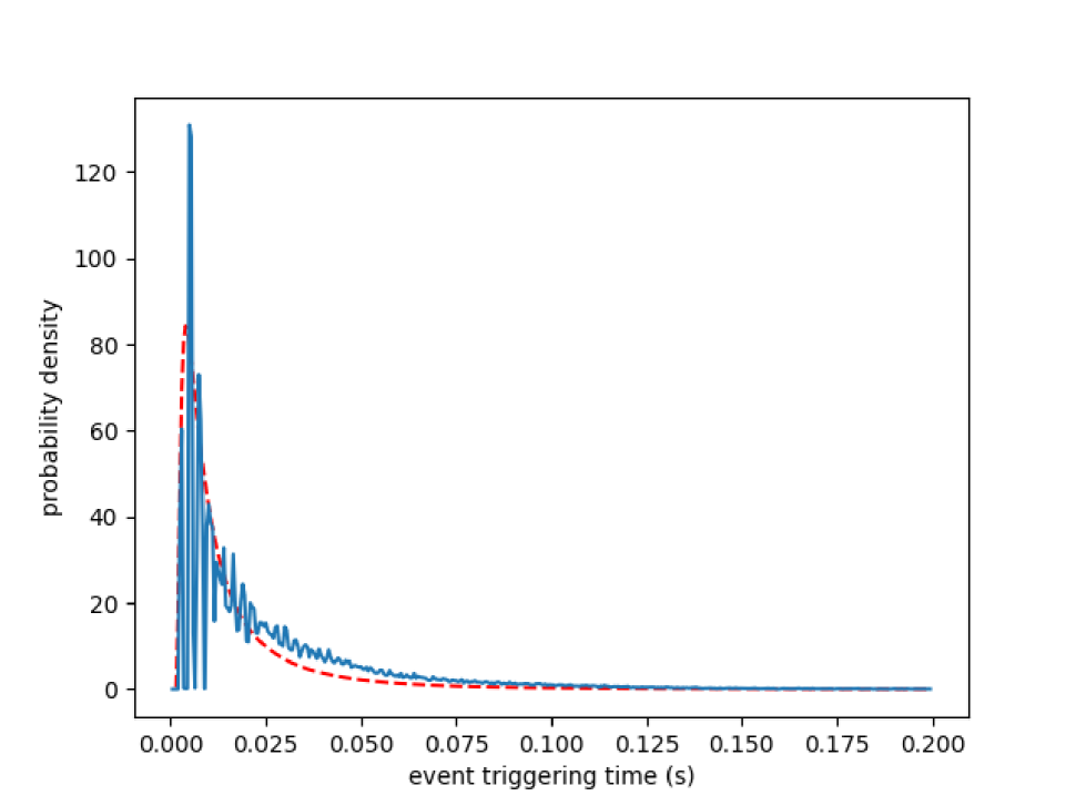


Fig. 3 shows the statistical distributions of event triggering time as the histograms with blue lines in different conditions. The fitting curves above the histograms, marked as red dashed lines, roughly follow the inverse Gaussian distribution. As is exemplified in Fig. 4, there exists significant discontinuity in the histograms, which is also shown in Fig. 3. It validates the existence of the time delay between consecutive triggering events caused by charge and discharge of parasitic capacitor of photodiode .

In Fig. 3, the lengths of discontinuity remain the same in each row but vary in each column, which demonstrates that the time delay only depends on rather than current light intensity . Therefore, the time delay follows a non-first-order behavior.
| current light intensity | ||||||
| 10 | 20 | 30 | 40 | 50 | ||
| light changing speed | 50 | |||||
| 60 | ||||||
| 70 | ||||||
| 80 | ||||||
| 90 | ||||||
| 100 | ||||||
| 150 | ||||||
| 200 | ||||||
The time delay is measured on the first discontinuous region, as can be seen in Fig. 4. Because it is more accurate compared with others that are influenced by the unstable changing speed of light.
We also evaluate the discontinuity length quantitatively in Table 2. The time delay declines with the increasing of changing speed , which can also be seen in Fig. 3. Furthermore, the product of and is almost unchanged with the light intensity . It proves our analysis of the inversely proportional relation between them.
The time delay exists with a non-first-order behavior, unlike the usual manner of first-order system of DVS. In the dim light conditions, the changing speed of light is slow because the absolute difference of light is small. As a result, the time delay is more significant.
4 CONCLUSIONS
In this paper, we study on the properties of DVS circuit, and find a new behavior of DVS: the time delay and discontinuity of event triggering time. It leads to a non-first-order behavior, different from the usual manners of DVS. The time delay is inversely proportional to the changing speed of light. In dim light conditions, the difference of light intensity is small, slowing the light variation. As a result, the time delay and discontinuity become prominent in dim light conditions. The experimental results are also provided for validation.
References
- [1] T. Delbruck and C.A. Mead, “Adaptive photoreceptor with wide dynamic range,” in Proceedings of IEEE International Symposium on Circuits and Systems-ISCAS’94. IEEE, 1994, vol. 4, pp. 339–342.
- [2] J.H. Lee, P.K.J. Park, C.-W. Shin, H. Ryu, B.C. Kang, and T. Delbruck, “Touchless hand gesture ui with instantaneous responses,” in 2012 IEEE International Conference on Image Processing. IEEE, 2012, pp. 1957–1960.
- [3] T. Delbruck, C. Li, R. Graca, and B. Mcreynolds, “Utility and feasibility of a center surround event camera,” in 2022 IEEE International Conference on Image Processing. IEEE, 2022, pp. 381–385.
- [4] Patrick Lichtsteiner, Christoph Posch, and Tobi Delbruck, “A 128 128 120 db 15 s latency asynchronous temporal contrast vision sensor,” IEEE Journal of Solid-State Circuits, vol. 43, no. 2, pp. 566–576, 2008.
- [5] G. Gallego, T. Delbrück, G. Orchard, C. Bartolozzi, B. Taba, A. Censi, S. Leutenegger, A.J. Davison, J. Conradt, K. Daniilidis, and D. Scaramuzza, “Event-based vision: A survey,” IEEE Transactions on Pattern Analysis and Machine Intelligence, vol. 44, no. 1, pp. 154–180, 2022.
- [6] M.A Mahowald, “Silicon retina with adaptive photoreceptors,” in Visual information processing: from neurons to chips. SPIE, 1991, vol. 1473, pp. 52–58.
- [7] G. Indiveri, B. Linares-Barranco, T.J. Hamilton, André Van S., R. Etienne-Cummings, T. Delbruck, S.-C. Liu, P. Dudek, P. Häfliger, S. Renaud, et al., “Neuromorphic silicon neuron circuits,” Frontiers in neuroscience, vol. 5, pp. 9202, 2011.
- [8] M. Muglikar, M. Gehrig, D. Gehrig, and D. Scaramuzza, “How to calibrate your event camera,” in Proceedings of the IEEE/CVF Conference on Computer Vision and Pattern Recognition, 2021, pp. 1403–1409.
- [9] T. Brewer and M. Hawks, “A comparative evaluation of the fast optical pulse response of event-based cameras,” in Image Sensing Technologies: Materials, Devices, Systems, and Applications VIII. SPIE, 2021, vol. 11723, pp. 86–103.
- [10] E. Mueggler, H. Rebecq, G. Gallego, T. Delbruck, and D. Scaramuzza, “The event-camera dataset and simulator: Event-based data for pose estimation, visual odometry, and slam,” The International Journal of Robotics Research, vol. 36, no. 2, pp. 142–149, 2017.
- [11] D. Gehrig, M. Gehrig, J. Hidalgo-Carrió, and D. Scaramuzza, “Video to events: Recycling video datasets for event cameras,” in Proceedings of the IEEE/CVF Conference on Computer Vision and Pattern Recognition, 2020, pp. 3586–3595.
- [12] Y. Hu, S.-C. Liu, and T. Delbruck, “v2e: From video frames to realistic dvs events,” in Proceedings of the IEEE/CVF Conference on Computer Vision and Pattern Recognition, 2021, pp. 1312–1321.
- [13] Rui Graca and Tobi Delbruck, “Unraveling the paradox of intensity-dependent dvs pixel noise,” arXiv preprint arXiv:2109.08640, 2021.
- [14] S. Lin, Y. Ma, Z. Guo, and B. Wen, “Dvs-voltmeter: Stochastic process-based event simulator for dynamic vision sensors,” in European Conference on Computer Vision. Springer, 2022, pp. 578–593.
- [15] M. Dentan and B. de Cremoux, “Numerical simulation of the nonlinear response of a pin photodiode under high illumination,” Journal of Lightwave Technology, vol. 8, no. 8, pp. 1137–1144, 1990.
- [16] B. Razavi, Fundamentals of microelectronics, John Wiley & Sons, 2021.
- [17] R. Graça, B. McReynolds, and T. Delbruck, “Shining light on the dvs pixel: A tutorial and discussion about biasing and optimization,” in Proceedings of the IEEE/CVF Conference on Computer Vision and Pattern Recognition, 2023, pp. 4044–4052.
- [18] H. Jiang, D. Sun, V. Jampani, M.-H. Yang, E. Learned-Miller, and J. Kautz, “Super slomo: High quality estimation of multiple intermediate frames for video interpolation,” in Proceedings of the IEEE conference on computer vision and pattern recognition, 2018, pp. 9000–9008.
- [19] H. Rebecq, D. Gehrig, and D. Scaramuzza, “Esim: an open event camera simulator,” in Conference on robot learning. PMLR, 2018, pp. 969–982.
- [20] B Series, “Colour gamut conversion from recommendation itu-r bt. 2020 to recommendation itu-r bt. 709,” International Telecommunication Union, 2017.