Bit-Exact ECC Recovery (BEER):
Determining DRAM On-Die ECC Functions
by Exploiting DRAM Data Retention Characteristics
Abstract
Increasing single-cell DRAM error rates have pushed DRAM manufacturers to adopt on-die error-correction coding (ECC), which operates entirely within a DRAM chip to improve factory yield. The on-die ECC function and its effects on DRAM reliability are considered trade secrets, so only the manufacturer knows precisely how on-die ECC alters the externally-visible reliability characteristics. Consequently, on-die ECC obstructs third-party DRAM customers (e.g., test engineers, experimental researchers), who typically design, test, and validate systems based on these characteristics.
To give third parties insight into precisely how on-die ECC transforms DRAM error patterns during error correction, we introduce Bit-Exact ECC Recovery (BEER), a new methodology for determining the full DRAM on-die ECC function (i.e., its parity-check matrix) without hardware tools, prerequisite knowledge about the DRAM chip or on-die ECC mechanism, or access to ECC metadata (e.g., error syndromes, parity information). BEER exploits the key insight that non-intrusively inducing data-retention errors with carefully-crafted test patterns reveals behavior that is unique to a specific ECC function.
We use BEER to identify the ECC functions of 80 real LPDDR4 DRAM chips with on-die ECC from three major DRAM manufacturers. We evaluate BEER’s correctness in simulation and performance on a real system to show that BEER is effective and practical across a wide range of on-die ECC functions. To demonstrate BEER’s value, we propose and discuss several ways that third parties can use BEER to improve their design and testing practices. As a concrete example, we introduce and evaluate BEEP, the first error profiling methodology that uses the known on-die ECC function to recover the number and bit-exact locations of unobservable raw bit errors responsible for observable post-correction errors.
1 Introduction
Dynamic random access memory (DRAM) is the predominant choice for system main memory across a wide variety of computing platforms due to its favorable cost-per-bit relative to other memory technologies. DRAM manufacturers maintain a competitive advantage by improving raw storage densities across device generations. Unfortunately, these improvements largely rely on process technology scaling, which causes serious reliability issues that reduce factory yield. DRAM manufacturers traditionally mitigate yield loss using post-manufacturing repair techniques such as row/column sparing [51]. However, continued technology scaling in modern DRAM chips requires stronger error-mitigation mechanisms to remain viable because of random single-bit errors that are increasingly frequent at smaller process technology nodes [120, 76, 129, 39, 99, 119, 133, 89, 160, 109, 127, 124]. Therefore, DRAM manufacturers have begun to use on-die error correction coding (on-die ECC), which silently corrects single-bit errors entirely within the DRAM chip [120, 76, 39, 129, 138]. On-die ECC is completely invisible outside of the DRAM chip, so ECC metadata (i.e., parity-check bits, error syndromes) that is used to correct errors is hidden from the rest of the system.
Prior works [60, 129, 120, 147, 133, 97, 98, 138] indicate that existing on-die ECC codes are 64- or 128-bit single-error correction (SEC) Hamming codes [44]. However, each DRAM manufacturer considers their on-die ECC mechanism’s design and implementation to be highly proprietary and ensures not to reveal its details in any public documentation, including DRAM standards [68, 69], DRAM datasheets [63, 149, 121, 158], publications [133, 97, 98, 76], and industry whitepapers [120, 147].
Because the unknown on-die ECC function is encapsulated within the DRAM chip, it obfuscates raw bit errors (i.e., pre-correction errors)111We use the term “error” to refer to any bit-flip event, whether observed (e.g., uncorrectable bit-flips) or unobserved (e.g., corrected by ECC). in an ECC-function-specific manner. Therefore, the locations of software-visible uncorrectable errors (i.e., post-correction errors) often no longer match those of the pre-correction errors that were caused by physical DRAM error mechanisms. While this behavior appears desirable from a black-box perspective, it poses serious problems for third-party DRAM customers who study, test and validate, and/or design systems based on the reliability characteristics of the DRAM chips that they buy and use. Section 2.2 describes these customers and the problems they face in detail, including, but not limited to, three important groups: (1) system designers who need to ensure that supplementary error-mitigation mechanisms (e.g., rank-level ECC within the DRAM controller) are carefully designed to cooperate with the on-die ECC function [160, 129, 40], (2) large-scale industries (e.g., computing system providers such as Microsoft [33], HP [47], and Intel [59], DRAM module manufacturers [92, 159, 4]) or government entities (e.g., national labs [131, 150]) who must understand DRAM reliability characteristics when validating DRAM chips they buy and use, and (3) researchers who need full visibility into physical device characteristics to study and model DRAM reliability [42, 43, 72, 172, 31, 178, 82, 138, 86, 109, 46, 84, 83, 85, 78, 80, 79, 81, 17, 20, 139].
For each of these third parties, merely knowing or reverse-engineering the type of ECC code (e.g., -bit Hamming code) based on existing industry [133, 97, 98, 120, 147, 60] and academic [129, 138] publications is not enough to determine exactly how the ECC mechanism obfuscates specific error patterns. This is because an ECC code of a given type can have many different implementations based on how its ECC function (i.e., its parity-check matrix) is designed, and different designs lead to different reliability characteristics. For example, Figure 1 shows the relative probability of observing errors in different bit positions for three different ECC codes of the same type (i.e., single-error correction Hamming code with 32 data bits and 6 parity-check bits) but that use different ECC functions. We obtain this data by simulating ECC words using the EINSim simulator [138, 2] and show medians and 95% confidence intervals calculated via statistical bootstrapping [32] over 1000 samples. We simulate a 0xFF test pattern222Other patterns show similar behavior, including RANDOM data. with uniform-random pre-correction errors at a raw bit error rate of (e.g., as often seen in experimental studies [43, 76, 109, 102, 157, 20, 46, 17, 139]).
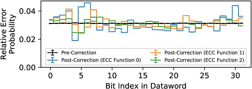
The data demonstrates that ECC codes of the same type can have vastly different post-correction error characteristics. This is because each ECC mechanism acts differently when faced with more errors than it can correct (i.e., uncorrectable errors), causing it to mistakenly perform ECC-function-specific “corrections” to bits that did not experience errors (i.e., miscorrections, which Section 3.3 expands upon). Therefore, a researcher or engineer who studies two DRAM chips that use the same type of ECC code but different ECC functions may find that the chips’ software-visible reliability characteristics are quite different even if the physical DRAM cells’ reliability characteristics are identical. On the other hand, if we know the full ECC function (i.e., its parity-check matrix), we can calculate exactly which pre-correction error pattern(s) result in a set of observed errors. Figure 1 is a result of aggregating such calculations across error patterns333Capturing approximately of the unique patterns., and Section 7.1 demonstrates how we can use the ECC function to infer pre-correction error counts and locations using only observed post-correction errors.
Knowing the precise transformation between pre- and post-correction errors benefits all of the aforementioned third-party use cases because it provides system designers, test engineers, and researchers with a way to isolate the error characteristics of the memory itself from the effects of a particular ECC function. Section 2.2 provides several example use cases and describes the benefits of knowing the ECC function in detail. While specialized, possibly intrusive methods (e.g., chip teardown [66, 164], advanced imaging techniques [48, 164]) can theoretically extract the ECC function, such techniques are typically inaccessible to or infeasible for many third-party users.
To enable third parties to reconstruct pre-correction DRAM reliability characteristics, our goal is to develop a methodology that can reliably and accurately determine the full on-die ECC function without requiring hardware tools, prerequisite knowledge about the DRAM chip or on-die ECC mechanism, or access to ECC metadata (e.g., error syndromes, parity information). To this end, we develop Bit-Exact ECC Recovery (BEER), a new methodology for determining a DRAM chip’s full on-die ECC function simply by studying the software-visible post-correction error patterns that it generates. Thus, BEER requires no hardware support, hardware intrusion, or access to internal ECC metadata (e.g., error syndromes, parity information). BEER exploits the key insight that forcing the ECC function to act upon carefully-crafted uncorrectable error patterns reveals ECC-function-specific behavior that disambiguates different ECC functions. BEER comprises three key steps: (1) deliberately inducing uncorrectable data-retention errors by pausing DRAM refresh while using carefully-crafted test patterns to control the errors’ bit-locations, which is done by leveraging data-retention errors’ intrinsic data-pattern asymmetry (discussed in Section 3.2), (2) enumerating the bit positions where the ECC mechanism causes miscorrections, and (3) using a SAT solver [28] to solve for the unique parity-check matrix that causes the observed set of miscorrections.
We experimentally apply BEER to 80 real LPDDR4 DRAM chips with on-die ECC from three major DRAM manufacturers to determine the chips’ on-die ECC functions. We describe the experimental steps required to apply BEER to any DRAM chip with on-die ECC and show that BEER tolerates observed experimental noise. We show that different manufacturers appear to use different on-die ECC functions while chips from the same manufacturer and model number appear to use the same on-die ECC function (Section 5.1.3). Unfortunately, our experimental studies with real DRAM chips have two limitations against further validation: (1) because the on-die ECC function is considered trade secret for each manufacturer, we are unable to obtain a groundtruth to compare BEER’s results against, even when considering non-disclosure agreements with DRAM manufacturers and (2) we are unable to publish the final ECC functions that we uncover using BEER for confidentiality reasons (discussed in Section 2.1).
To overcome the limitations of experimental studies with real DRAM chips, we rigorously evaluate BEER’s correctness in simulation (Section 6). We show that BEER correctly recovers the on-die ECC function for 115300 single-error correction Hamming codes444This irregular number arises from evaluating a different number of ECC functions for different code lengths because longer codes require exponentially more simulation time (discussed in Section 6.1)., which are representative of on-die ECC, with ECC word lengths ranging from 4 to 247 bits. We evaluate our BEER implementation’s runtime and memory consumption using a real system to demonstrate that BEER is practical and the SAT problem that BEER requires is realistically solvable.
To demonstrate how BEER is useful in practice, we propose and discuss several ways that third parties can leverage the ECC function that BEER reveals to more effectively design, study, and test systems that use DRAM chips with on-die ECC (Section 7). As a concrete example, we introduce and evaluate Bit-Exact Error Profiling (BEEP), a new DRAM data-retention error profiling methodology that reconstructs pre-correction error counts and locations purely from observed post-correction errors. Using the ECC function revealed by BEER, BEEP infers precisely which unobservable raw bit errors correspond to observed post-correction errors at a given set of testing conditions. We show that BEEP enables characterizing pre-correction errors across a wide range of ECC functions, ECC word lengths, error patterns, and error rates. We publicly release our tools as open-source software: (1) a new tool [1] for applying BEER to experimental data from real DRAM chips and (2) enhancements to EINSim [2] for evaluating BEER and BEEP in simulation.
This paper makes the following key contributions:
-
1.
We provide Bit-Exact ECC Recovery (BEER), the first methodology that determines the full DRAM on-die ECC function (i.e., its parity-check matrix) without requiring hardware tools, prerequisite knowledge about the DRAM chip or on-die ECC mechanism, or access to ECC metadata (e.g., error syndromes, parity information).
-
2.
We experimentally apply BEER to 80 real LPDDR4 DRAM chips with unknown on-die ECC mechanisms from three major DRAM manufacturers to determine their on-die ECC functions. We show that BEER is robust to observed experimental noise and that DRAM chips from different manufacturers appear to use different on-die ECC functions while chips from the same manufacturer and model number appear to use the same function.
-
3.
We evaluate BEER’s correctness in simulation and show that BEER correctly identifies the on-die ECC function for 115300 representative on-die ECC codes with ECC word lengths ranging from 4 to 247 bits.
-
4.
We analytically evaluate BEER’s experimental runtime and use a real system to measure the SAT solver’s performance and memory usage characteristics (e.g., negligible for short codes, median of 57.1 hours and 6.3 GiB memory for representative 128-bit codes, and up to 62 hours and 11.4 GiB memory for 247-bit codes) to show that BEER is practical.
-
5.
We propose and evaluate Bit-Exact Error Profiling (BEEP), a new DRAM data-retention error profiling methodology that uses a known ECC function (e.g., via BEER) to infer pre-correction error counts and locations. We show that BEEP enables characterizing the bit-exact pre-correction error locations across different ECC functions, codeword lengths, error patterns, and error rates.
- 6.
2 Challenges of Unknown On-Die ECCs
This section discusses why on-die ECC is considered proprietary, how its secrecy causes difficulties for third-party consumers, and how the BEER methodology helps overcome these difficulties by identifying the full on-die ECC function.
2.1 Secrecy Concerning On-Die ECC
On-die ECC silently mitigates increasing single-bit errors that reduce factory yield [120, 76, 129, 39, 99, 119, 133, 89, 160, 109, 127, 124]. Because on-die ECC is invisible to the external DRAM chip interface, older DRAM standards [69, 68] place no restrictions on the on-die ECC mechanism while newer standards [70] specify only a high-level description for on-die ECC to support new (albeit limited) DDR5 features, e.g., on-die ECC scrubbing. In particular, there are no restrictions on the design or implementation of the on-die ECC function itself.
This means that knowing an on-die ECC mechanism’s details could reveal information about its manufacturer’s factory yield rates, which are highly proprietary [55, 23] due to their direct connection with business interests, potential legal concerns, and competitiveness in a USD 45+ billion DRAM market [143, 170]. Therefore, manufacturers consider their on-die ECC designs and implementations to be trade secrets that they are unwilling to disclose. In our experience, DRAM manufacturers will not reveal on-die ECC details under confidentiality agreements, even for large-scale industry board vendors for whom knowing the details stands to be mutually beneficial.555Even if such agreements were possible, industry teams and academics without major business relations with DRAM manufacturers (i.e., an overwhelming majority of the potentially interested scientists and engineers) will likely be unable to secure disclosure.
This raises two challenges for our experiments with real DRAM chips: (1) we do not have access to “groundtruth” ECC functions to validate BEER’s results against and (2) we cannot publish the final ECC functions that we determine using BEER for confidentiality reasons based on our relationships with the DRAM manufacturers. However, this does not prevent third-party consumers from applying BEER to their own devices, and we hope that our work encourages DRAM manufacturers to be more open with their designs going forward.666While full disclosure would be ideal, a more realistic scenario could be more flexible on-die ECC confidentiality agreements. As recent work [35] shows, security or protection by obscurity is likely a poor strategy in practice.
2.2 On-Die ECC’s Impact on Third Parties
On-die ECC alters a DRAM chip’s software-visible reliability characteristics so that they are no longer determined solely by how errors physically occur within the DRAM chip. Figure 1 illustrates this by showing how using different on-die ECC functions changes how the same underlying DRAM errors appear to the end user. Instead of following the pre-correction error distribution (i.e., uniform-random errors), the post-correction errors exhibit ECC-function-specific shapes that are difficult to predict without knowing precisely which ECC function is used in each case. This means that two commodity DRAM chips with different on-die ECC functions may show similar or different reliability characteristics irrespective of how the underlying DRAM technology and error mechanisms behave. Therefore, the physical error mechanisms’ behavior alone can no longer explain a DRAM chip’s post-correction error characteristics.
Unfortunately, this poses a serious problem for third-party DRAM consumers (e.g., system designers, testers, and researchers), who can no longer accurately understand a DRAM chip’s reliability characteristics by studying its software-visible errors. This lack of understanding prevents third parties from both (1) making informed design decisions, e.g., when building memory-controller based error-mitigation mechanisms to complement on-die ECC and (2) developing new ideas that rely on on leveraging predictable aspects of a DRAM chip’ reliability characteristics, e.g., physical error mechanisms that are fundamental to all DRAM technology. As error rates worsen with continued technology scaling [120, 76, 129, 39, 99, 119, 133, 89, 86, 90, 124, 127], manufacturers will likely resort to stronger codes that further distort the post-correction reliability characteristics. The remainder of this section describes three key ways in which an unknown on-die ECC function hinders third-parties, and determining the function helps mitigate the problem.
Designing High-Reliability Systems. System designers often seek to improve memory reliability beyond that which the DRAM provides alone (e.g., by including rank-level ECC within the memory controllers of server-class machines or ECC within on-chip caches). In particular, rank-level ECCs are carefully designed to mitigate common DRAM failure modes [21] (e.g., chip failure [129], burst errors [116, 29]) in order to correct as many errors as possible. However, designing for key failure modes requires knowing a DRAM chip’s reliability characteristics, including the effects of any underlying ECC function (e.g., on-die ECC) [160, 40]. For example, Son et al. [160] show that if on-die ECC suffers an uncorrectable error and mistakenly “corrects” a non-erroneous bit (i.e., introduces a miscorrection), the stronger rank-level ECC may no longer be able to even detect what would otherwise be a detectable (possibly correctable) error. To prevent this scenario, both levels of ECC must be carefully co-designed to complement each others’ weaknesses. In general, high-reliability systems can be more effectively built around DRAM chips with on-die ECC if its ECC function and its effects on typical DRAM failure modes are known.
Testing, Validation, and Quality Assurance. Large-scale computing system providers (e.g., Microsoft [33], HP [47], Intel [59]), DRAM module manufacturers [92, 159, 4], and government entities (e.g., national labs [150, 131]) typically perform extensive third-party testing of the DRAM chips they purchase in order to ensure that the chips meet internal performance/energy/reliability targets. These tests validate that DRAM chips operate as expected and that there are well-understood, convincing root-causes (e.g., fundamental DRAM error mechanisms) for any observed errors. Unfortunately, on-die ECC interferes with two key components of such testing. First, it obfuscates the number and bit-exact locations of pre-correction errors, so diagnosing the root cause for any observed error becomes challenging. Second, on-die ECC encodes all written data into ECC codewords, so the values written into the physical cells likely do not match the values observed at the DRAM chip interface. The encoding process defeats carefully-constructed test patterns that target specific circuit-level phenomena (e.g., exacerbating interference between bitlines [3, 123, 79]) because the encoded data may no longer have the intended effect. Unfortunately, constructing such patterns is crucial for efficient testing since it minimizes the testing time required to achieve high error coverage [51, 3]. In both cases, the full on-die ECC function determined by BEER describes exactly how on-die ECC transforms pre-correction error patterns into post-correction ones. This enables users to infer pre-correction error locations (demonstrated in Section 7.1) and design test patterns that result in codewords with desired properties (discussed in Section 7.2).
Scientific Error-Characterization Studies. Scientific error-characterization studies explore physical DRAM error mechanisms (e.g., data retention [42, 43, 157, 75, 173, 172, 74, 79, 80, 78, 109, 139, 46, 81], reduced access-latency [17, 102, 104, 83, 85, 84, 37, 20, 16], circuit disturbance [90, 79, 136, 135, 86, 35, 81]) by deliberately exacerbating the error mechanism and analyzing the resulting errors’ statistical properties (e.g., frequency, spatial distribution). These studies help build error models [178, 43, 157, 31, 104, 20, 83, 94], leading to new DRAM designs and operating points that improve upon the state-of-the-art. Unfortunately, on-die ECC complicates error analysis and modeling by (1) obscuring the physical pre-correction errors that are the object of study and (2) preventing direct access to parity-check bits, thereby precluding comprehensive testing of all DRAM cells in a given chip. Although prior work [138] enables inferring high-level statistical characteristics of the pre-correction errors, it does not provide a precise mapping between pre-correction and post-correction errors, which is only possible knowing the full ECC function. Knowing the full ECC function, via our new BEER methodology, enables recovering the bit-exact locations of pre-correction errors throughout the entire ECC word (as we demonstrate in Section 7.1) so that error-characterization studies can separate the effects of DRAM error mechanisms from those of on-die ECC. Section 7 provides a detailed discussion of several key characterization studies that BEER enables.
3 Background
This section provides a basic overview of DRAM, coding theory, and satisfiability (SAT) solvers as pertinent to this manuscript. For further detail, we refer the reader to comprehensive texts on DRAM design and operation [77, 65, 54, 64, 45, 154, 155, 20, 17, 102, 180, 61, 18, 106, 103, 19, 111, 153], coding theory [115, 122, 148, 53, 146, 25, 108], and SAT solvers [28, 8, 24, 30].
3.1 DRAM Cells and Data Storage
A DRAM chip stores each data bit in its own storage cell using the charge level of a storage capacitor. Because the capacitor is susceptible to charge leakage [42, 169, 139, 110, 26, 95, 90, 109, 138], the stored value may eventually degrade to the point of data loss, resulting in a data-retention error. During normal DRAM operation, a refresh operation restores the data value stored in each cell every refresh window (), e.g., 32ms or 64ms [69, 68, 67, 109, 139, 110], to prevent data-retention errors.
Depending on a given chip’s circuit design, each cell may store data using one of two encoding conventions: a true-cell encodes data ‘1’ as a fully-charged storage capacitor (i.e., the CHARGED state), and an anti-cell encodes data ‘1’ as a fully-discharged capacitor (i.e., the DISCHARGED state). Although a cell’s encoding scheme is transparent to the rest of the system during normal operation, it becomes evident in the presence of data-retention errors because DRAM cells typically decay only from their CHARGED to their DISCHARGED state as shown experimentally by prior work [26, 95, 90, 109, 138, 139, 110].
3.2 Studying DRAM Errors
Deliberately inducing DRAM errors (e.g., by violating default timing parameters) reveals detailed information about a DRAM chip’s internal design through the resulting errors’ statistical characteristics. Prior works use custom memory testing platforms (e.g., FPGA-based [46]) and commodity CPUs [6, 57] (e.g., by changing CPU configuration registers via the BIOS [56]) to study a variety of DRAM error mechanisms, including data-retention [139, 110, 26, 95, 90, 109, 138], circuit timing violations [83, 104, 17, 102, 85, 84], and RowHammer [90, 125, 126, 86, 136, 135]. Our work focuses on data-retention errors because they exhibit well-studied properties that are helpful for our purposes:
-
1.
They are easily induced and controlled by manipulating the refresh window () and ambient temperature.
- 2.
- 3.
Off-DRAM-Chip Errors. Software-visible memory errors often occur due to failures in components outside the DRAM chip (e.g., sockets, buses) [119]. However, our work focuses on errors that occur within a DRAM chip, which are a serious and growing concern at modern technology node sizes [120, 76, 129, 39, 99, 119, 133, 89, 160, 124, 127]. These errors are the primary motivation for on-die ECC, which attempts to correct them before they are ever observed outside the DRAM chip.
3.3 On-Die ECC and Hamming Codes
As manufacturers continue to increase DRAM storage density, unwanted single-bit errors appear more frequently [105, 128, 129, 120, 76, 50, 41, 119, 162, 161, 114, 151, 138, 39, 99, 133, 89] and reduce factory yield. To combat these errors, manufacturers use on-die ECC [128, 129, 120, 76, 133, 39, 138], which is an error-correction code implemented directly in the DRAM chip.
Figure 2 shows how a system might interface with a memory chip that uses on-die ECC. The system writes -bit datawords () to the chip, which internally maintains an expanded -bit representation of the data called a codeword (), created by the ECC encoding of d. The stored codeword may experience errors, resulting in a potentially erroneous codeword (). If more errors occur than ECC can correct, e.g., two errors in a single-error correction (SEC) code, the final dataword read out after ECC decoding () may also contain errors. The encoding and decoding functions are labeled and .
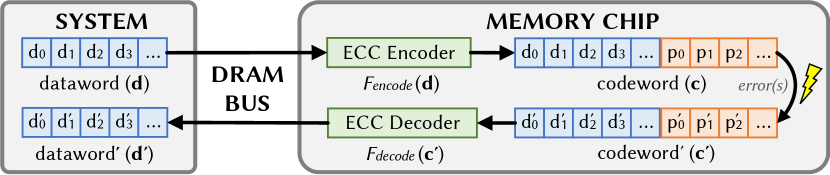
For all linear codes (e.g., SEC Hamming codes [44]), and can be represented using matrix transformations. As a demonstrative example throughout this paper, we use the (7, 4, 3) Hamming code [44] shown in Equation 1. represents a generator matrix such that the codeword is computed from the dataword as .
| (1) |
Decoding. The most common decoding algorithm is known as syndrome decoding, which simply computes an error syndrome that describes if and where an error exists:
-
•
: no error detected.
-
•
: error detected, and describes its bit-exact location.
Note that the error syndrome computation is unaware of the true error count; it blindly computes the error syndrome(s) assuming a low probability of uncorrectable errors. If, however, an uncorrectable error is present (e.g., deliberately induced during testing), one of three possibilities may occur:
-
•
Silent data corruption: syndrome is zero; no error.
-
•
Partial correction: syndrome points to one of the errors.
-
•
Miscorrection: syndrome points to a non-erroneous bit.
When a nonzero error syndrome occurs, the ECC decoding logic simply flips the bit pointed to by the error syndrome, potentially exacerbating the overall number of errors.
Design Space. Each manufacturer can freely select and functions, whose implementations can help to meet a set of design constraints (e.g., circuit area, reliability, power consumption). The space of functions that a designer can choose from is quantified by the number of arrangements of columns of . This means that for an -bit code with data bits, there are possible ECC functions. Section 4.2 formalizes this space of possible functions in the context of our work.
3.4 Boolean Satisfiability (SAT) Solvers
Satisfiability (SAT) solvers [28, 8, 24, 30, 38, 140] find possible solutions to logic equation(s) with one or more unknown Boolean variables. A SAT solver accepts one or more such equations as inputs, which effectively act as constraints over the unknown variables. The SAT solver then attempts to determine a set of values for the unknown variables such that the equations are satisfied (i.e., the constraints are met). The SAT solver will return either (1) one (of possibly many) solutions or (2) no solution if the Boolean equation is unsolvable.
4 Determining the ECC Function
BEER identifies an unknown ECC function by systematically reconstructing its parity-check matrix based on the error syndromes that the ECC logic generates while correcting errors. Different ECC functions compute different error syndromes for a given error pattern, and by constructing and analyzing carefully-crafted test cases, BEER uniquely identifies which ECC function a particular implementation uses. This section describes how and why this process works. Section 5 describes how BEER accomplishes this in practice for on-die ECC.
4.1 Disambiguating Linear Block Codes
DRAM ECCs are linear block codes, e.g., Hamming codes [44] for on-die ECC [60, 129, 120, 147, 133, 97, 98, 138], BCH [9, 49] or Reed-Solomon [145] codes for rank-level ECC [26, 87], whose encoding and decoding operations are described by linear transformations of their respective inputs (i.e., and matrices, respectively). We can therefore determine the full ECC function by independently determining each of its linear components.
We can isolate each linear component of the ECC function by injecting errors in each codeword bit position and observing the resulting error syndromes. For example, an -bit Hamming code’s parity-check matrix can be systematically determined by injecting a single-bit error in each of the bit positions: the error syndrome that the ECC decoder computes for each pattern is exactly equal to the column of the parity-check matrix that corresponds to the position of the injected error. As an example, Equation 2 shows how injecting an error at position 2 (i.e., adding error pattern to codeword ) extracts the corresponding column of the parity-check matrix in the error syndrome . By the definition of a block code, for all codewords [27, 53], so isolates column 2 of (i.e., ).
| (2) |
Thus, the entire parity-check matrix can be fully determined by testing across all 1-hot error patterns. Cojocar et al. [26] use this approach on DRAM rank-level ECC, injecting errors into codewords on the DDR bus and reading the resulting error syndromes provided by the memory controller.
4.2 Determining the On-Die ECC Function
Unfortunately, systematically determining an ECC function as described in Section 4.1 is not possible with on-die ECC for two key reasons. First, on-die ECC’s parity-check bits cannot be accessed directly, so we have no easy way to inject an error within them. Second, on-die ECC does not signal an error-correction event or report error syndromes (i.e., ). Therefore, even if specialized methods (e.g., chip teardown [66, 164], advanced imaging techniques [48, 164]) could inject errors within a DRAM chip package where the on-die ECC mechanism resides,777Such methods may reveal the exact on-die ECC circuitry. However, they are typically inaccessible to or infeasible for many third-party consumers. the error syndromes would remain invisible, so the approach taken by Cojocar et al. [26] cannot be applied to on-die ECC. To determine the on-die ECC function using the approach of Section 4.1, we first formalize the unknown on-die ECC function and then determine how we can infer error syndromes within the constraints of the formalized problem.
4.2.1 Formalizing the Unknown ECC Function
We assume that on-die ECC uses a systematic encoding, which means that the ECC function stores data bits unmodified. This is a reasonable assumption for real hardware since it greatly simplifies data access [181] and is consistent with our experimental results in Section 5.1.2. Furthermore, because the DRAM chip interface exposes only data bits, the relative ordering of parity-check bits within the codeword is irrelevant from the system’s perspective. Mathematically, the different choices of bit positions represent equivalent codes that all have identical error-correction properties and differ only in their internal representations [146, 148], which on-die ECC does not expose. Therefore, we are free to arbitrarily choose the parity-check bit positions within the codeword without loss of generality. If it becomes necessary to identify the exact ordering of bits within the codeword (e.g., to infer circuit-level implementation details), reverse-engineering techniques based on physical DRAM error mechanisms [104, 73] can potentially be used.
A systematic encoding and the freedom to choose parity-check bit positions mean that we can assume that the ECC function is in standard form, where we express the parity-check matrix for an code as a partitioned matrix . is a conventional notation for the sub-matrix that corresponds to information bit positions and is an identity matrix that corresponds to parity-check bit positions. Note that the example ECC code of Equation 1 is in standard form. With this representation, all codewords take the form , where and are data and parity-check symbols, respectively.
4.2.2 Identifying Syndromes Using Miscorrections
Given that on-die ECC conceals error syndromes, we develop a new approach for determining the on-die ECC function that indirectly determines error syndromes based on how the ECC mechanism responds when faced with uncorrectable errors. To induce uncorrectable errors, we deliberately pause normal DRAM refresh operations long enough (e.g., several minutes at 80∘C) to cause a large number of data-retention errors (e.g., BER ) throughout a chip. These errors expose a significant number of miscorrections in different ECC words, and the sheer number of data-retention errors dominates any unwanted interference from other possible error mechanisms (e.g., particle strikes [117]).
To control which data-retention errors occur, we write carefully-crafted test patterns that restrict the errors to specific bit locations. This is possible because only cells programmed to the CHARGED state can experience data-retention errors as discussed in Section 3.2. By restricting pre-correction errors to certain cells, if a post-correction error is observed in an unexpected location, it must be an artifact of error correction, i.e., a miscorrection. Such a miscorrection is significant since it: (1) signals an error-correction event, (2) is purely a function of the ECC decoding logic, and (3) indirectly reveals the error syndrome generated by the pre-correction error pattern. The indirection occurs because, although the miscorrection does not expose the raw error syndrome, it does reveal that whichever error syndrome is generated internally by the ECC logic exactly matches the parity-check matrix column that corresponds to the position of the miscorrected bit.
These three properties mean that miscorrections are a reliable tool for analyzing ECC functions: for a given pre-correction error pattern, different ECC functions will generate different error syndromes, and therefore miscorrections, depending on how the functions’ parity-check matrices are organized. This means that a given ECC function causes miscorrections only within certain bits, and the locations of miscorrection-susceptible bits differ between functions. Therefore, we can differentiate ECC functions by identifying which miscorrections are possible for different test patterns.
4.2.3 Identifying Useful Test Patterns
To construct a set of test patterns that suffice to uniquely identify an ECC function, we observe that a miscorrection is possible in a DISCHARGED data bit only if the bit’s error syndrome can be produced by some linear combination of the parity-check matrix columns that correspond to CHARGED bit locations. For example, consider the 1-CHARGED patterns that each set one data bit to the CHARGED state and all others to the DISCHARGED state. In these patterns, data-retention errors may only occur in either (1) the CHARGED bit or (2) any parity-check bits that the ECC function also sets to the CHARGED state. With these restrictions, observable miscorrections may only occur within data bits whose error syndromes can be created by some linear combination of the parity-check matrix columns that correspond to the CHARGED cells within the codeword.
As a concrete example, consider the codeword of Equation 3. C and D represent that the corresponding cell is programmed to the CHARGED and DISCHARGED states, respectively.
| (3) |
Because only CHARGED cells can experience data-retention errors, there are possible error syndromes that correspond to the unique combinations of CHARGED cells failing. Table 1 illustrates these eight possibilities.
A miscorrection occurs whenever the error syndrome of an uncorrectable error pattern matches the parity-check matrix column of a non-erroneous data bit. In this case, the column’s location would then correspond to the bit position of the miscorrection. However, a miscorrection only reveals information if it occurs within one of the DISCHARGED data bits, for only then are we certain that the observed bit flip is unambiguously a miscorrection rather than an uncorrected data-retention error. Therefore, the test patterns we use should maximize the number of DISCHARGED bits so as to increase the number of miscorrections that yield information about the ECC function.
To determine which test patterns to use, we expand upon the approach of injecting 1-hot errors described in Section 4.1. Although we would need to write data to all codeword bits in order to test every 1-hot error pattern, on-die ECC does not allow writing directly to the parity-check bits. This leads to two challenges. First, we cannot test 1-hot error patterns for which the 1-hot error is within the parity-check bits, which means that we cannot differentiate ECC functions that differ only within their parity-check bit positions. Fortunately, this is not a problem because, as Section 4.2.1 discusses in detail, all such functions are equivalent codes with identical externally-visible error-correction properties. Therefore, we are free to assume that the parity-check matrix is in standard form, which specifies parity-check bits’ error syndromes (i.e., ) and obviates the need to experimentally determine them.
Second, writing the bits of the dataword with a single CHARGED cell results in a codeword with an unknown number of CHARGED cells because the ECC function independently determines the values of remaining parity-check bits. As a result, the final codeword may contain anywhere from to CHARGED cells, and the number of CHARGED cells will vary for different test patterns. Because we cannot directly access the parity-check bits’ values, we do not know which cells are CHARGED for a given test pattern, and therefore, we cannot tie post-correction errors back to particular pre-correction error patterns. Fortunately, we can work around this problem by considering all possible error patterns that a given codeword can experience, which amounts to examining all combinations of errors that the CHARGED cells can experience. Table 1 illustrates this for when the dataword is programmed with a 1-CHARGED test pattern (as shown in Equation 3). In this example, the encoded codeword contains three CHARGED cells, which may experience any of possible error patterns. Section 5.1.3 discusses how we can accomplish testing all possible error patterns in practice by exploiting the fact that data-retention errors occur uniform-randomly, so testing across many different codewords provides samples from many different error patterns at once.
4.2.4 Shortened Codes
Linear block codes can be either of full-length if all possible error syndromes are present within the parity-check matrix (e.g., all error syndromes for a Hamming code with parity-check bits, as is the case for the code shown in Equation 1) or shortened if one or more information symbols are truncated while retaining the same number of parity-check symbols [27, 53]. This distinction is crucial for determining appropriate test patterns because, for full-length codes, the 1-CHARGED patterns identify the miscorrection-susceptible bits for all possible error syndromes. In this case, testing additional patterns that have more than one CHARGED bit provides no new information because any resulting error syndromes are already tested using the 1-CHARGED patterns.
However, for shortened codes, the 1-CHARGED patterns may not provide enough information to uniquely identify the ECC function because the 1-CHARGED patterns can no longer test for the missing error syndromes. Fortunately, we can recover the missing information by reconstructing the truncated error syndromes using pairwise combinations of the 1-CHARGED patterns. For example, asserting two CHARGED bits effectively tests an error syndrome that is the linear combination of the bits’ corresponding parity-check matrix columns. Therefore, by supplementing the 1-CHARGED patterns with the 2-CHARGED patterns, we effectively encompass the error syndromes that were shortened. Section 6.1 evaluates BEER’s sensitivity to code length, showing that the 1-CHARGED patterns are indeed sufficient for full-length codes and the {1,2}-CHARGED patterns for shortened codes that we evaluate with dataword lengths between 4 and 247.
5 Bit-Exact Error Recovery (BEER)
Our goal in this work is to develop a methodology that reliably and accurately determines the full ECC function (i.e., its parity-check matrix) for any DRAM on-die ECC implementation without requiring hardware tools, prerequisite knowledge about the DRAM chip or on-die ECC mechanism, or access to ECC metadata (e.g., error syndromes, parity information). To this end, we present BEER, which systematically determines the ECC function by observing how it reacts when subjected to carefully-crafted uncorrectable error patterns. BEER implements the ideas developed throughout Section 4 and consists of three key steps: (1) experimentally inducing miscorrections, (2) analyzing observed post-correction errors, and (3) solving for the ECC function.
This section describes each of these steps in detail in the context of experiments using 32, 20, and 28 real LPDDR4 DRAM chips from three major manufacturers, whom we anonymize for confidentiality reasons as A, B, and C, respectively. We perform all tests using a temperature-controlled infrastructure with precise control over the timings of refresh and other DRAM bus commands.
5.1 Step 1: Inducing Miscorrections
To induce miscorrections as discussed in Section 4.2.3, we must first identify the (1) CHARGED and DISCHARGED encodings of each cell and (2) layout of individual datawords within the address space. This section describes how we determine these in a way that is applicable to any DRAM chip.
5.1.1 Determining CHARGED and DISCHARGED States
We determine the encodings of the CHARGED and DISCHARGED states by experimentally measuring the layout of true- and anti-cells throughout the address space as done in prior works [90, 95, 138]. We write data ‘0’ and data ‘1’ test patterns to the entire chip while pausing DRAM refresh for 30 minutes at temperatures between C. The resulting data-retention error patterns reveal the true- and anti-cell layout since each test pattern isolates one of the cell types. We find that chips from manufacturers A and B use exclusively true-cells, and chips from manufacturer C use 50%/50% true-/anti-cells organized in alternating blocks of rows with block lengths of 800, 824, and 1224 rows. These observations are consistent with the results of similar experiments performed by prior work [138].
5.1.2 Determining the Layout of Datawords
To determine which addresses correspond to individual ECC datawords, we program one cell per row888We assume that ECC words do not straddle row boundaries since accesses would then require reading two rows simultaneously. However, one cell per bank can be tested to accommodate this case if required. to the CHARGED state with all other cells DISCHARGED. We then sweep the refresh window from 10 seconds to 10 minutes at C to induce uncorrectable errors. Because only CHARGED cells can fail, post-correction errors may only occur in bit positions corresponding to either (1) the CHARGED cell itself or (2) DISCHARGED cells due to a miscorrection. By sweeping the bit position of the CHARGED cell within the dataword, we observe miscorrections that are restricted exclusively to within the same ECC dataword. We find that chips from all three manufacturers use identical ECC word layouts: each contiguous 32B region of DRAM comprises two 16B ECC words that are interleaved at byte granularity. A 128-bit dataword is consistent with prior industry and academic works on on-die ECC [97, 98, 120, 138].
5.1.3 Testing With 1,2-CHARGED Patterns
To test each of the 1- or 2-CHARGED patterns, we program an equal number of datawords with each test pattern. For example, a 128-bit dataword yields and 1- and 2-CHARGED test patterns, respectively. As Section 4.2.3 discusses, BEER must identify all possible miscorrections for each test pattern. To do so, BEER must exercise all possible error patterns that a codeword programmed with a given test pattern can experience (e.g., up to unique error patterns for a (136, 128) Hamming code using a 2-CHARGED pattern).
Fortunately, although BEER must test a large number of error patterns, even a single DRAM chip typically contains millions of ECC words (e.g., 128-bit words for a 16 Gib chip), and we simultaneously test them all when we reduce the refresh window across the entire chip. Because data-retention errors occur uniform-randomly (discussed in Section 3.2), every ECC word tested provides an independent sample of errors. Therefore, even one experiment provides millions of samples of different error patterns within the CHARGED cells, and running multiple experiments at different operating conditions (e.g., changing temperature or the refresh window) across multiple DRAM chips999Assuming chips of the same model use the same on-die ECC mechanism, which our experimental results in Section 5.1.3 support. dramatically increases the sample size, making the probability of not observing a given error pattern exceedingly low.. We analyze experimental runtime in Section 6.3.
Table 2 illustrates testing the 1-CHARGED patterns using the ECC function given by Equation 1. There are four test patterns, and Table 2 shows the miscorrections that are possible for each one assuming that all cells are true cells. For this ECC function, miscorrections are possible only for test pattern 0, and no pre-correction error pattern exists that can cause miscorrections for the other test patterns. Note that, for errors in the CHARGED-bit positions, we cannot be certain whether a post-correction error is a miscorrection or simply a data-retention error, so we label it using ‘?’. We refer to the cumulative pattern-miscorrection pairs as a miscorrection profile. Thus, Table 2 shows the miscorrection profile of the ECC function given by Equation 1.
| 1-CHARGED Pattern ID | 1-CHARGED Pattern | Possible Miscorrections |
|---|---|---|
| (Bit-Index of CHARGED Cell) | ||
| 3 | ||
| 2 | ||
| 1 | ||
| 0 |
To obtain the miscorrection profile of the on-die ECC function within each DRAM chip that we test, we lengthen the refresh window to between 2 minutes, where uncorrectable errors begin to occur frequently (BER ), and 22 minutes, where nearly all ECC words exhibit uncorrectable errors (BER ), in 1 minute intervals at 80∘C. During each experiment, we record which bits are susceptible to miscorrections for each test pattern (analogous to Table 2). Figure 3 shows this information graphically, giving the logarithm of the number of errors observed in each bit position (-axis) for each 1-CHARGED test pattern (-axis). The data is taken from the true-cell regions of a single representative chip from each manufacturer. Errors in the CHARGED bit positions (i.e., where ) stand out clearly because they occur alongside all miscorrections as uncorrectable errors.
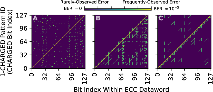
The data shows that miscorrection profiles vary significantly between different manufacturers. This is likely because each manufacturer uses a different parity-check matrix: the possible miscorrections for a given test pattern depend on which parity-check matrix columns are used to construct error syndromes. With different matrices, different columns combine to form different error syndromes. The miscorrection profiles of manufacturers B and C exhibit repeating patterns, which likely occur due to regularities in how syndromes are organized in the parity-check matrix, whereas the matrix of manufacturer A appears to be relatively unstructured. We suspect that manufacturers use different ECC functions because each manufacturer employs their own circuit design, and specific parity-check matrix organizations lead to more favorable circuit-level tradeoffs (e.g., layout area, critical path lengths).
We find that chips of the same model number from the same manufacturer yield identical miscorrection profiles, which (1) validates that we are observing design-dependent data and (2) confirms that chips from the same manufacturer and product generation appear to use the same ECC functions. To sanity-check our results, we use EINSim [138, 2] to simulate the miscorrection profiles of the final parity-check matrices we obtain from our experiments with real chips, and we observe that the miscorrection profiles obtained via simulation match those measured via real chip experiments.
5.2 Step 2: Analyzing Post-Correction Errors
In practice, BEER may either (1) fail to observe a possible miscorrection or (2) misidentify a miscorrection due to unpredictable transient errors (e.g., soft errors from particle strikes, variable-retention time errors, voltage fluctuations). These events can theoretically pollute the miscorrection profile with incorrect data, potentially resulting in an illegal miscorrection profile, i.e., one that does not match any ECC function.
Fortunately, case (1) is unlikely given the sheer number of ECC words even a single chip provides for testing (discussed in Section 5.1.3). While it is possible that different ECC words throughout a chip use different ECC functions, we believe that this is unlikely because it complicates the design with no clear benefits. Even if a chip does use more than one ECC function, the different functions will likely follow patterns aligning with DRAM substructures (e.g., alternating between DRAM rows or subarrays [91, 83]), and we can test each region individually.
Similarly, case (2) is unlikely because transient errors occur randomly and rarely [141] as compared with the data-retention error rates that we induce for BEER (), so transient error occurrence counts are far lower than those of real miscorrections that are observed frequently in miscorrection-susceptible bit positions. Therefore, we apply a simple threshold filter to remove rarely-observed post-correction errors from the miscorrection profile. Figure 4 shows the relative probability of observing a miscorrection in each bit position aggregated across all 1-CHARGED test patterns for a representative chip from manufacturer B. Each data point is a boxplot that shows the full distribution of probability values, i.e., min, median, max, and interquartile-range (IQR), observed when sweeping the refresh window from 2 to 22 minutes (i.e., the same experiments described in Section 5.1.3).
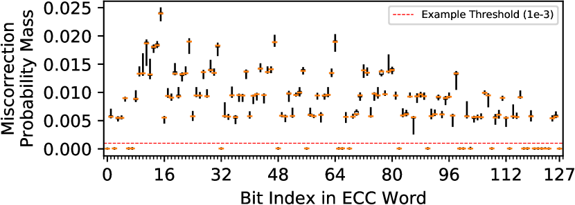
We see that zero and nonzero probabilities are distinctly separated, so we can robustly resolve miscorrections for each bit. Furthermore, each distribution is extremely tight, meaning that any of the individual experiments (i.e., any single component of the distributions) is suitable for identifying miscorrections. Therefore, a simple threshold filter (illustrated in Figure 4) distinctly separates post-correction errors that occur near-zero times from miscorrections that occur significantly more often.
5.3 Step 3: Solving for the ECC Function
We use the Z3 SAT solver [28] (described in Section 3.4) to identify the exact ECC function given a miscorrection profile. To determine the encoding () and decoding () functions, we express them as unknown generator (G) and parity-check (H) matrices, respectively. We then add the following constraints to the SAT solver for G and H:
-
1.
Basic linear code properties (e.g., unique H columns).
-
2.
Standard form matrices, as described in Section 4.2.1.
-
3.
Information contained within the miscorrection profile (i.e., pattern can(not) yield a miscorrection in bit ).
Upon evaluating the SAT solver with these constraints, the resulting G and H matrices represent the ECC encoding and decoding functions, respectively, that cause the observed miscorrection profile. To verify that no other ECC function may result in the same miscorrection profile, we simply repeat the SAT solver evaluation with the additional constraint that the already discovered G and H matrices are invalid. If the SAT solver finds another ECC function that satisfies the new constraints, the solution is not unique.
To seamlessly apply BEER to the DRAM chips that we test, we develop an open-source C++ application [1] that incorporates the SAT solver and determines the ECC function corresponding to an arbitrary miscorrection profile. The tool exhaustively searches for all possible ECC functions that satisfy the aforementioned constraints and therefore will generate the input miscorrection profile. Using this tool, we apply BEER to miscorrection profiles that we experimentally measure across all chips using refresh windows up to 30 minutes and temperatures up to 80∘C. We find that BEER uniquely identifies the ECC function for all manufacturers. Unfortunately, we are unable to publish the resulting ECC functions for confidentiality reasons as set out in Section 2.1. Although we are confident in our results because our SAT solver tool identifies a unique ECC function that explains the observed miscorrection profiles for each chip, we have no way to validate BEER’s results against a groundtruth. To overcome this limitation, we demonstrate BEER’s correctness using simulation in Section 6.1.
5.4 Requirements and Limitations
Although we demonstrate BEER’s effectiveness using both experiment and simulation, BEER has several testing requirements and limitations that we review in this section.
Testing Requirements
-
•
Single-level ECC: BEER assumes that there is no second level of ECC (e.g., rank-level ECC in the DRAM controller) present during testing.101010We can potentially extend BEER to multiple levels of ECC by extending the SAT problem to the concatenated code formed by the combined ECCs and constructing test patterns that target each level sequentially, but we leave this direction to future work. This is reasonable since system-level ECCs can typically be bypassed (e.g., via FPGA-based testing or disabling through the BIOS) or reverse-engineered [26], even in the presence of on-die ECC, before applying BEER.
-
•
Inducing data-retention errors: BEER requires finding a refresh window (i.e., ) for each chip that is long enough to induce data-retention errors and expose miscorrections. Fortunately, we find that refresh windows between 1-30 minutes at 80∘C reveal more than enough miscorrections to apply BEER. In general, the refresh window can be easily modified (discussed in Section 3.2), and because data-retention errors are fundamental to DRAM technology, BEER applies to all DDRx DRAM families regardless of their data access protocols and will likely hold for future DRAM chips, whose data-retention error rates will likely be even more prominent [120, 76, 129, 39, 99, 119, 133, 89, 160, 109].
Limitations
-
•
ECC code type: BEER works on systematic linear block codes, which are commonly employed for latency-sensitive main memory chips since: (i) they allow the data to be directly accessed without additional operations [181] and (ii) stronger codes (e.g., LDPC [36], concatenated codes [34]) cost considerably more area and latency [11, 132].
-
•
No groundtruth: BEER alone cannot confirm whether the ECC function that it identifies is the correct answer. However, if BEER finds exactly one ECC function that explains the experimentally observed miscorrection profile, it is very likely that the ECC function is correct.
-
•
Disambiguating equivalent codes: On-die ECC does not expose the parity-check bits, so BEER can only determine the ECC function to an equivalent code (discussed in Sections 4.2.1 and 4.2.3). Fortunately, equivalent codes differ only in their internal metadata representations, so this limitation should not hinder most third-party studies. In general, we are unaware of any way to disambiguate equivalent codes without accessing the ECC mechanism’s internals.
6 BEER Evaluation
We evaluate BEER’s correctness in simulation, SAT solver performance on a real system, and experimental runtime analytically. Our evaluations both (1) show that BEER is practical and correctly identifies the ECC function within our simulation-based analyses, and (2) provide intuition for how the SAT problem’s complexity scales for longer ECC codewords.
6.1 Simulation-Based Correctness Evaluation
We simulate applying BEER to DRAM chips with on-die ECC using a modified version of the EINSim [138, 2] open-source DRAM error-correction simulator that we also publicly release [2]. We simulate 115300 single-error correction Hamming code functions that are representative of those used for on-die ECC [60, 129, 120, 147, 133, 97, 98, 138]: 2000 each for dataword lengths between 4 and 57 bits, 100 each between 58 and 120 bits, and 100 each for selected values between 121 and 247 bits because longer codes require significantly more simulation time. For each ECC function, we simulate inducing data-retention errors within the 1-, 2-, and 3-CHARGED111111We include the 3-CHARGED patterns to show that they fail to uniquely identify all ECC functions despite comprising combinatorially more test patterns than the combined 1- and 2-CHARGED patterns. test patterns according to the data-retention error properties outlined in Section 3.2. For each test pattern, we model a real experiment by simulating ECC words and data-retention error rates ranging from to to obtain a miscorrection profile. Then, we apply BEER to the miscorrection profiles and show that BEER correctly recovers the original ECC functions.
Figure 5 shows how many unique ECC functions BEER finds when using different test patterns to generate miscorrection profiles. For each dataword length tested, we show the minimum, median, and maximum number of solutions identified across all miscorrection profiles. The data shows that BEER is always able to recover the original unique ECC function using the {1,2}-CHARGED configuration that uses both the 1-CHARGED and 2-CHARGED test patterns. For full-length codes (i.e., with dataword lengths ) that contain all possible error syndromes within the parity-check matrix by construction, all test patterns uniquely determine the ECC function, including the 1-CHARGED patterns alone.
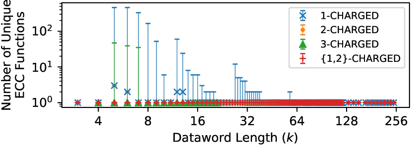
On the other hand, the individual 1-, 2-, and 3-CHARGED patterns sometimes identify multiple ECC functions for shortened codes, with more solutions identified both for (1) shorter codes and (2) codes with more aggressive shortening. However, the data shows that BEER often still uniquely identifies the ECC function even using only the 1-CHARGED patterns (i.e., for 87.7% of all codes simulated) and always does so with the {1,2}-CHARGED patterns. This is consistent with the fact that shortened codes expose fewer error syndromes to test (discussed in Section 4.2.3). It is important to note that, even if BEER identifies multiple solutions, it still narrows a combinatorial-sized search space to a tractable number of ECC functions that are well suited to more expensive analyses (e.g., intrusive error-injection, die imaging techniques, or manual inspection).
While our simulations do not model interference from transient errors, such errors are rare events [141] when compared with the amount of uncorrectable data-retention errors that BEER induces. Even if sporadic transient errors were to occur, Section 5.2 discusses in detail how BEER mitigates their impact on the miscorrection profile using a simple thresholding filter.
6.2 Real-System Performance Evaluation
We evaluate BEER’s performance and memory usage using ten servers with 24-core 2.30 GHz Intel Xeon(R) Gold 5118 CPUs [58] and 192 GiB 2666 MHz DDR4 DRAM [68] each. All measurements are taken with Hyper-Threading [58] enabled and all cores fully occupied. Figure 6 shows overall runtime and memory usage when running BEER with the 1-CHARGED patterns for different ECC code lengths on a log-log plot along with the time required to (1) solve for the ECC function (“Determine Function”) and (2) verify the uniqueness of the solution (“Check Uniqueness”). Each data point gives the minimum, median, and maximum values observed across our simulated ECC functions (described in Section 6.1). We see that the total runtime and memory usage are negligible for short codes and grow as large as 62 hours and 11.4 GiB of memory for large codes. For a representative dataword length of 128 bits, the median total runtime and memory usage are 57.1 hours and 6.3 GiB, respectively. At each code length where we add an additional parity-check bit, the runtime and memory usage jump accordingly since the complexity of the SAT evaluation problem increases by an extra dimension.
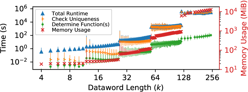
The total runtime is quickly dominated by the SAT solver checking uniqueness, which requires exhaustively exploring the entire search space of a given ECC function. However, simply determining the solution ECC function(s) is much faster, requiring less than 2.7 minutes even for the longest codes evaluated and for shortened codes that potentially have multiple solutions using only the 1-CHARGED patterns. From this data, we conclude that BEER is practical for reasonable-length codes used for on-die ECC (e.g., ). However, our BEER implementation has room for optimization, e.g., using dedicated GF(2) BLAS libraries (e.g., LELA [52]) or advanced SAT solver theories (e.g., SMT bitvectors [10]), and an optimized implementation would likely improve performance, enabling BEER’s application to an even greater range of on-die ECC functions. Section 7.3 discusses such optimizations in greater detail. Nevertheless, BEER is a one-time offline process, so it need not be aggressively performant in most use-cases.
6.3 Analytical Experiment Runtime Analysis
Our experimental runtime is overwhelmingly bound by waiting for data-retention errors to occur during a lengthened refresh window (e.g., 10 minutes) while interfacing with the DRAM chip requires only on the order of milliseconds (e.g., 168 ms to read an entire 2 GiB LPDDR4-3200 chip [69]). Therefore, we estimate total experimental runtime as the sum of the refresh windows that we individually test. For the data we present in Section 5.1.3, testing each refresh window between 2 to 22 minutes in 1 minute increments requires a combined 4.2 hours of testing for a single chip. However, if chips of the same model number use the same ECC functions (as our data supports in Section 5.1.3), we can reduce overall testing latency by parallelizing individual tests across different chips. Furthermore, because BEER is likely a one-time exercise for a given DRAM chip, it is sufficient that BEER is practical offline.
7 Example Practical Use-Cases
BEER empowers third-party DRAM users to decouple the reliability characteristics of modern DRAM chips from any particular on-die ECC function that a chip implements. This section discusses five concrete analyses that BEER enables. To our knowledge, BEER is the first work capable of inferring this information without bypassing the on-die ECC mechanism. We hope that end users and future works find more ways to extend and apply BEER in practice.
7.1 BEEP: Profiling for Raw Bit Errors
We introduce Bit-Exact Error Profiling (BEEP), a new data-retention error profiling algorithm enabled by BEER that infers the number and bit-exact locations of pre-correction error-prone cells when given a set of operating conditions that cause uncorrectable errors in an ECC word. To our knowledge, BEEP is the first DRAM error profiling methodology capable of identifying bit-exact error locations throughout the entire on-die ECC codeword, including within the parity bits.
7.1.1 BEEP: Inference Based on Miscorrections
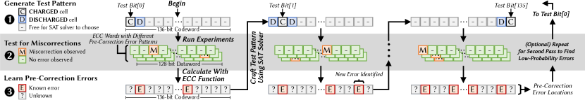
Because miscorrections are purely a function of the ECC logic (discussed in Section 4.2.2), an observed miscorrection indicates that a specific pre-correction error pattern has occurred. Although several such patterns can map to the same miscorrection, BEEP narrows down the possible pre-correction error locations by using the known parity-check matrix (after applying BEER) to construct test patterns for additional experiments that disambiguate the possibilities. At a high level, BEEP crafts test patterns to reveal errors as it incrementally traverses each codeword bit, possibly using multiple passes to capture low-probability errors. As BEEP iterates over the codeword, it builds up a list of suspected error-prone cells.
BEEP comprises three phases: crafting suitable test patterns, experimental testing with crafted patterns, and calculating pre-correction error locations from observed miscorrections. Figure 7 illustrates these three phases in an example where BEEP profiles for pre-correction errors in a 128-bit ECC dataword. The following sections explain each of the three phases and refer to Figure 7 as a running example.
7.1.2 Crafting Suitable Test Patterns
Conventional DRAM error profilers (e.g., [169, 110, 109, 79, 104, 139, 81, 22, 165, 95, 46, 71]) use carefully designed test patterns that induce worst-case circuit conditions in order to maximize their coverage of potential errors [3, 123]. Unfortunately, on-die ECC encodes all data into codewords, so the intended software-level test patterns likely do not maintain their carefully-designed properties when written to the physical DRAM cells. BEEP circumvents these ECC-imposed restrictions by using a SAT solver along with the known ECC function (via BEER) to craft test patterns that both (1) locally induce the worst-case circuit conditions and (2) result in observable miscorrections if suspected error-prone cells do indeed fail.
Without loss of generality, we assume that the worst-case conditions for a given bit occur when its neighbors are programmed with the opposite charge states, which prior work shows to exacerbate circuit-level coupling effects and increase error rates [3, 109, 79, 123, 166, 144, 5, 156, 93, 107, 130]. If the design of a worst-case pattern is not known, or if it has a different structure than we assume, BEEP can be adapted by simply modifying the relevant SAT solver constraints (described below). To ensure that BEEP observes a miscorrection when a given error occurs, BEEP crafts a pattern that will suffer a miscorrection if the error occurs alongside an already-discovered error. We express these conditions to the SAT solver using the following constraints:
-
1.
Bits adjacent to the target bit have opposing charge states.
-
2.
One or more miscorrections is possible using some combination of the already-identified data-retention errors.
Several such patterns typically exist, and BEEP simply uses the first one that the SAT solver returns (although a different BEEP implementation could test multiple patterns to help identify low-probability errors). Figure 7 illustrates how such a test pattern appears physically within the cells of a codeword: the target cell is CHARGED, its neighbors are DISCHARGED, and the SAT solver freely determines the states of the remaining cells to increase the likelihood of a miscorrection if the target cell fails. If the SAT solver fails to find such a test pattern, BEEP attempts to craft a pattern using constraint 2 alone, which, unlike constraint 1, is essential to observing miscorrections. Failing that, BEEP simply skips the bit until more error-prone cells are identified that could facilitate causing miscorrections. We evaluate how successfully BEEP identifies errors in Section 7.1.4, finding that a second pass over the codeword helps in cases of few or low-probability errors.
7.1.3 Experimental Testing with Crafted Patterns
BEEP tests a pattern by writing it to the target ECC word, inducing errors by lengthening the refresh window, and reading out the post-correction data. Figure 7 shows examples of post-correction error patterns that might be observed during an experiment. Each miscorrection indicates that an uncorrectable number of pre-correction errors exists, and BEEP uses the parity-check matrix H to calculate their precise locations. This is possible because each miscorrection reveals an error syndrome for the (unknown) erroneous pre-correction codeword that caused the miscorrection. Therefore, we can directly solve for as shown in Equation 4.
| (4) |
This is a system of equations with one equation for each of unknowns, i.e., one each for the inaccessible parity bits. There is guaranteed to be exactly one solution for since the parity-check matrix always has full rank (i.e., ). Since we also know the original codeword (), we can simply compare the two (i.e., ) to determine the bit-exact error pattern that led to the observed miscorrection. Figure 7 shows how BEEP updates a list of learned pre-correction error locations, which the SAT solver then uses to construct test patterns for subsequent bits. Once all bits are tested, the list of pre-correction errors yields the number and bit-locations of all identified error-prone cells.
7.1.4 Evaluating BEEP’s Success Rate
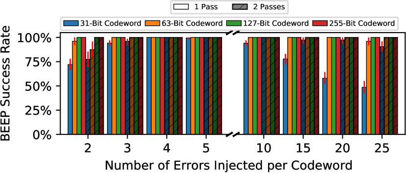
To understand how BEEP performs in practice, we evaluate its success rate, i.e., the likelihood that BEEP correctly identifies errors within a codeword. We use a modified version of EINSim [2] to perform Monte-Carlo simulation across 100 codewords per measurement. To keep our analysis independent of any particular bit-error rate model, we subdivide experiments by the number of errors () injected per codeword. In this way, we can flexibly evaluate the success rate for a specific error distribution using the law of total probability over the s.
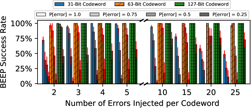
Number of Passes. Figure 8 shows BEEP’s success rate when using one and two passes over the codeword for different codeword lengths. Each bar shows the median value over the 100 codewords with an error bar showing the 5th and 95th percentiles. The data shows that BEEP is highly successful across all tested error counts, especially for longer 127- and 255-bit codewords that show a 100% success rate even with a single pass. Longer codewords perform better in part because BEEP uses one test pattern per bit, which means that longer codes lead to more patterns. However, longer codewords perform better even with comparable test-pattern counts (e.g., 2 passes with 31-bit vs 1 pass with 63-bit codewords) because longer codewords simply have more bits (and therefore, error syndromes) for the SAT solver to consider when crafting a miscorrection-prone test pattern. On the other hand, miscorrection-prone test patterns are more difficult to construct for shorter codes that provide fewer bits to work with, so BEEP fails more often when testing shorter codes.
Per-Bit Error Probabilities. Figure 9 shows how BEEP’s success rate changes using a single pass when the injected errors have different per-bit probabilities of error (P[error]). This experiment represents a more realistic scenario where some DRAM cells probabilistically experience data-retention errors. We see that BEEP remains effective (i.e., has a near-100% success rate) for realistic 63- and 127-bit codeword lengths, especially at higher bit-error probabilities and error counts. BEEP generally has a higher success rate with longer codes compared to shorter ones, and for shorter codewords at low error probabilities, the data shows that BEEP may require more test patterns (e.g., multiple passes) to reliably identify all errors.
It is important to note that, while evaluating low error probabilities is demonstrative, it represents a pessimistic scenario since a real DRAM chip exhibits a mix of low and high per-bit error probabilities.121212Patel et al. [139] provide a preliminary exploration of how per-bit error probabilities are distributed throughout a DRAM chip, but formulating a detailed error model for accurate simulation is beyond the scope of our work. Although any error-profiling mechanism that identifies errors based on when they manifest might miss low-probability errors,131313Patel et al. [139] increase error coverage by exacerbating the bit-error probability, and their approach (REAPER) can be used alongside BEEP to help identify low-probability errors. the data shows that BEEP is resilient to low error probabilities, especially for longer, more realistic codewords. Therefore, our evaluations demonstrate that BEEP effectively enables a new profiling methodology that uses the ECC function determined by BEER to infer pre-correction errors from observed post-correction error patterns.
7.1.5 Other DRAM Error Mechanisms
Although we demonstrate BEEP solely for data-retention errors, BEEP can potentially be extended to identify errors that occur due to other DRAM error mechanisms (e.g., stuck-at faults, circuit timing failures). However, simultaneously diagnosing multiple error models is a very difficult problem since different types of faults can be nearly indistinguishable (e.g., data-retention errors and stuck-at-DISCHARGED errors). Profiling for arbitrary error types is a separate problem from what we tackle in this work, and we intend BEEP as a simple, intuitive demonstration of how knowing the ECC function is practically useful. Therefore, we leave extending BEEP to alternative DRAM error mechanisms to future work.
7.2 Other Use-Cases that Benefit from BEER
We identify four additional use cases for which BEER mitigates on-die ECC’s interference with third-party studies by revealing the full ECC function (i.e., its parity-check matrix).
7.2.1 Combining Error Mitigation Mechanisms
If the on-die ECC function is known, a system architect can design a second level of error mitigation (e.g., rank-level ECC) that better suits the error characteristics of a DRAM chip with on-die ECC. Figure 1 provides a simple example of how different ECC functions cause different data bits to be more error-prone even though the pre-correction errors are uniformly distributed. This means that on-die ECC changes the DRAM chip’s software-visible error characteristics in a way that depends on the particular ECC function it employs. If the on-die ECC function is known, we can calculate the expected post-correction error characteristics141414By assuming a given data value distribution, e.g., fixed values for a predictable software application, uniform-random data for a general system. and build an error model that accounts for the transformative effects of on-die ECC. Using this error model, the system architect can make an informed decision when selecting a secondary mitigation mechanism to complement on-die ECC. For example, architects could modify a traditional rank-level ECC scheme to asymmetrically protect certain data bits that are more prone to errors than others as a result of on-die ECC’s behavior [95, 174]. In general, BEER enables system designers to better design secondary error-mitigation mechanisms to suit the expected DRAM reliability characteristics, thereby improving overall system reliability.
7.2.2 Crafting Targeted Test Patterns
Several DRAM error mechanisms are highly pattern sensitive, including RowHammer [90, 125, 126, 86], data-retention [139, 109, 110, 78, 79, 81, 43, 88], and reduced-access-latency [83, 104, 102, 17, 20]. Different test patterns affect error rates by orders of magnitude [100, 109, 139, 86, 81, 79, 80] because each pattern exercises different static and dynamic circuit-level effects. Therefore, test patterns are typically designed carefully to induce the worst-case circuit conditions for the error mechanism under test (e.g., marching ‘1’s [3, 109, 139, 46, 123]). As Section 7.1.2 discusses in greater detail, on-die ECC restricts the possible test patterns to only the ECC function’s codewords. Fortunately, the SAT-solver-based approach that BEEP uses to craft test patterns generalizes to crafting targeted test patterns for these error mechanisms also.
7.2.3 Studying Spatial Error Distributions
Numerous prior works [157, 90, 17, 136, 104, 83, 20] experimentally study the spatial distributions of errors throughout the DRAM chip in order to gain insight into how the chip operates and how its performance, energy, and/or reliability can be improved. These studies rely on inducing errors at relatively high error rates so that many errors occur that can leak information about a device’s underlying structure. With on-die ECC, studying spatial error distributions requires identifying pre-correction errors throughout the codeword, including within the inaccessible parity bits. BEEP demonstrates one possible concrete way by which BEER enables these studies for chips with on-die ECC.
7.2.4 Diagnosing Post-Correction Errors
A third-party tester may want to determine the physical reason(s) behind an observed error. For example, a system integrator who is validating a DRAM chip’s worst-case operating conditions may observe unexpected errors due to an unforeseen defect (e.g., at a precise DQ-pin position). Unfortunately, on-die ECC obscures both the number and locations of pre-correction errors, so the observed errors no longer provide insight into the underlying physical error mechanism responsible. Using BEEP, such errors can be more easily diagnosed because the revealed pre-correction errors directly result from the error mechanism.
7.3 Extensions and Future Work
Our work demonstrates that on-die ECC is not an insurmountable problem for third-party system design and testing. To further explore how tools like BEER can help clarify a DRAM chip’s core reliability characteristics, we identify several ways in which future studies can build upon our work. We believe these are promising directions to explore and will further facilitate studying the reliability characteristics of current and future devices with on-die ECC.
Extension to Other Devices. BEER theoretically applies to any memory device that uses a linear block code in which we can exploit data-dependent errors (e.g., CHARGED-to-DISCHARGED) to control which miscorrections occur. A concrete example is DRAM with rank-level ECC, where BEER can be applied as is.151515There may be no need to infer error syndromes from miscorrections if the CPU directly exposes them [26]. However, BEER may be extensible to other memory devices (e.g., Flash memory [11, 13, 14, 112, 113, 12, 118], STT-MRAM [62, 182, 96], PCM [142, 101, 177, 152], Racetrack [179, 137], RRAM [176, 134, 171]) if its core principles can be adapted for their error models and ECC functions. These memories all exhibit reliability challenges that BEER can help third-party scientists and engineers better tackle and overcome.
Further Constraining the SAT Problem. We believe there are several ways to further constrain the SAT problem, including (i) prioritizing more likely hardware ECC implementations, (ii) adding additional SAT constraints for obvious or trivial cases, and (iii) further constraining the set of test patterns.
Improving SAT Solver Efficiency. Our implementations of BEER and BEEP express ECC arithmetic (e.g., GF(2) matrix operations, SAT constraints) using simple Boolean logic equations. An optimized implementation that leverages native GF(2) BLAS libraries (e.g., LELA [52]) and advanced SAT solver theories (e.g., SMT bitvectors [10]) could drastically improve BEER’s performance, enabling BEER for a wider variety of ECC functions. Taking this a step further, future work could reformulate BEER’s SAT problem mathematically in order to directly solve for the parity-check matrix that can produce a given miscorrection profile. Such an approach could identify the solution significantly faster than using a SAT solver to perform a brute-force exploration of the entire solution space.
8 Related Work
To our knowledge, this is the first work to (i) determine the full on-die ECC function and (ii) recover the number and bit-exact error locations of pre-correction errors in DRAM chips with on-die ECC without any insight into the ECC mechanism or any hardware modification. We distinguish BEER from related works that study on-die ECC, techniques for reverse-engineering DRAM ECC functions, and DRAM error profiling.
On-Die ECC. Several works study on-die ECC [129, 138, 15, 40], but only Patel et al. [138] attempt to identify pre-correction error characteristics without bypassing or modifying the on-die ECC mechanism. Although Patel et al. [138] statistically infer high-level characteristics about the ECC mechanism and pre-correction errors, their approach has several key limitations (discussed in Section 1). BEER overcomes these limitations and identifies (1) the full ECC function and (2) the bit-exact locations of pre-correction errors without requiring any prerequisite knowledge about the errors being studied.
Determining ECC Functions. Prior works reverse-engineer ECC characteristics in Flash memories [167, 168, 175], DRAM with rank-level ECC [26], and on-die ECC [138]. However, none of these works can identify the full ECC function by studying data only at the external DRAM chip interface because they either require (1) examining the encoded data [167, 168, 175], (2) injecting errors directly into the codeword [26], or (3) knowing when an ECC correction is performed and obtaining the resulting error syndrome [26]. On-die ECC provides no insight into the error-correction process and does not report if or when a correction is performed.
DRAM Error Profiling. Prior work proposes many DRAM error profiling methodologies [42, 43, 157, 75, 173, 172, 74, 79, 80, 78, 46, 104, 83, 85, 37, 20, 169, 110, 109, 141, 139, 84, 102, 90, 17, 86, 26, 95, 138]. Unfortunately, none of these approaches are capable of identifying pre-correction error locations throughout the entire codeword (i.e., including within parity-check bits).
9 Conclusion
We introduce Bit-Exact Error Recovery (BEER), a new methodology for determining the full DRAM on-die ECC function (i.e., its parity-check matrix) without requiring hardware support, prerequisite knowledge about the DRAM chip or on-die ECC mechanism, or access to ECC metadata (e.g., parity-check bits, error syndromes). We use BEER to determine the on-die ECC functions of 80 real LPDDR4 DRAM chips and show that BEER is both effective and practical using rigorous simulations. We discuss five concrete use-cases for BEER, including BEEP, a new DRAM error profiling methodology capable of inferring exact pre-correction error counts and locations. We believe that BEER takes an important step towards enabling effective third-party design and testing around DRAM chips with on-die ECC and are hopeful that BEER will enable many new studies going forward.
Acknowledgments
We thank the SAFARI Research Group members for the valuable input and stimulating intellectual environment they provide, Karthik Sethuraman for his expertise in nonparametric statistics, and the anonymous reviewers for their feedback.
References
- [1] “BEER Source Code,” https://github.com/CMU-SAFARI/BEER.
- [2] “EINSim Source Code,” https://github.com/CMU-SAFARI/EINSim.
- [3] R. D. Adams, High Performance Memory Testing: Design Principles, Fault Modeling and Self-Test. Springer SBM, 2002.
- [4] ADATA, “ADATA XPG DDR4 Officially Validated by AMD as AM4/Ryzen Compatible,” ADATA, Tech. Rep., 2017.
- [5] Z. Al-Ars, S. Hamdioui, and A. J. van de Goor, “Effects of Bit Line Coupling on the Faulty Behavior of DRAMs,” in VTS, 2004.
- [6] AMD, “AMD Opteron 4300 Series Processors,” 2018.
- [7] S. Baek, S. Cho, and R. Melhem, “Refresh Now and Then,” in TC, 2014.
- [8] N. Bjørner, A.-D. Phan, and L. Fleckenstein, “nu-Z: An Optimizing SMT Solver,” in TACAS, 2015.
- [9] R. C. Bose and D. K. Ray-Chaudhuri, “On a Class of Error Correcting Binary Group Codes,” Information and Control, 1960.
- [10] R. Brummayer and A. Biere, “Boolector: An Efficient SMT Solver for Bit-Vectors and Arrays,” in International Conference on Tools and Algorithms for the Construction and Analysis of Systems, 2009.
- [11] Y. Cai, S. Ghose, E. F. Haratsch, Y. Luo, and O. Mutlu, “Error Characterization, Mitigation, and Recovery In Flash-Memory-Based Solid-State Drives,” Proc. IEEE, 2017.
- [12] Y. Cai, S. Ghose, E. F. Haratsch, Y. Luo, and O. Mutlu, “Errors in Flash-Memory-Based Solid-State Drives: Analysis, Mitigation, and Recovery,” Inside Solid State Drives, 2018.
- [13] Y. Cai, E. F. Haratsch, O. Mutlu, and K. Mai, “Error Patterns in MLC NAND Flash Memory: Measurement, Characterization, and Analysis,” in DATE, 2012.
- [14] Y. Cai, G. Yalcin, O. Mutlu, E. F. Haratsch, A. Cristal, O. S. Unsal, and K. Mai, “Error Analysis and Retention-Aware Error Management for NAND Flash Memory,” in ITJ, 2013.
- [15] S. Cha et al., “Defect Analysis and Cost-Effective Resilience Architecture for Future DRAM Devices,” in HPCA, 2017.
- [16] K. Chandrasekar, S. Goossens, C. Weis, M. Koedam, B. Akesson, N. Wehn, and K. Goossens, “Exploiting Expendable Process-Margins in DRAMs for Run-Time Performance Optimization,” in DATE, 2014.
- [17] K. K. Chang, A. Kashyap, H. Hassan, S. Ghose, K. Hsieh, D. Lee, T. Li, G. Pekhimenko, S. Khan, and O. Mutlu, “Understanding Latency Variation in Modern DRAM Chips: Experimental Characterization, Analysis, and Optimization,” in SIGMETRICS, 2016.
- [18] K. K. Chang, D. Lee, Z. Chishti, A. R. Alameldeen, C. Wilkerson, Y. Kim, and O. Mutlu, “Improving DRAM Performance by Parallelizing Refreshes with Accesses,” in HPCA, 2014.
- [19] K. K. Chang, P. J. Nair, D. Lee, S. Ghose, M. K. Qureshi, and O. Mutlu, “Low-Cost Inter-Linked Subarrays (LISA): Enabling Fast Inter-Subarray Data Movement in DRAM,” in HPCA, 2016.
- [20] K. K. Chang, A. G. Yağlıkçı, S. Ghose, A. Agrawal, N. Chatterjee, A. Kashyap, D. Lee, M. O’Connor, H. Hassan, and O. Mutlu, “Understanding Reduced-Voltage Operation in Modern DRAM Devices: Experimental Characterization, Analysis, and Mechanisms,” in SIGMETRICS, 2017.
- [21] H.-M. Chen, S.-Y. Lee, T. Mudge, C.-J. Wu, and C. Chakrabarti, “Configurable-ECC: Architecting a Flexible ECC Scheme to Support Different Sized Accesses in High Bandwidth Memory Systems,” TC, 2018.
- [22] K.-L. Cheng, M.-F. Tsai, and C.-W. Wu, “Neighborhood Pattern-Sensitive Fault Testing and Diagnostics for Random-Access Memories,” TCAD, 2002.
- [23] B. R. Childers, J. Yang, and Y. Zhang, “Achieving Yield, Density and Performance Effective DRAM at Extreme Technology Sizes,” in MEMSYS, 2015.
- [24] A. Cimatti, A. Franzén, A. Griggio, R. Sebastiani, and C. Stenico, “Satisfiability Modulo The Theory of Costs: Foundations and Applications,” in TACAS, 2010.
- [25] G. C. Clark Jr and J. B. Cain, Error-Correction Coding for Digital Communications. Springer SBM, 2013.
- [26] L. Cojocar, K. Razavi, C. Giuffrida, and H. Bos, “Exploiting Correcting Codes: On the Effectiveness of ECC Memory Against Rowhammer Attacks,” in S&P, 2019.
- [27] D. J. Costello and S. Lin, Error Control Coding: Fundamentals and Applications. Prentice Hall, 1982.
- [28] L. De Moura and N. Bjørner, “Z3: An Efficient SMT Solver,” in TACAS, 2008.
- [29] T. J. Dell, “A White Paper on the Benefits of Chipkill-Correct ECC for PC Server Main Memory,” IBM Microelectronics Division, 1997.
- [30] I. Dillig, T. Dillig, K. L. McMillan, and A. Aiken, “Minimum Satisfying Assignments for SMT,” in CAV, 2012.
- [31] N. Edri, P. Meinerzhagen, A. Teman, A. Burg, and A. Fish, “Silicon-Proven, Per-Cell Retention Time Distribution Model for Gain-Cell Based eDRAMs,” IEEE TOCS, 2016.
- [32] B. Efron, “Bootstrap Methods: Another Look at the Jackknife,” in Breakthroughs in Statistics, 1992.
- [33] S. Field, “Microsoft Azure uses Error-Correcting Code Memory for Enhanced Reliability and Security,” https://azure.microsoft.com/en-us/blog/microsoft-azure-uses-error-correcting-code-memory-for-enhanced-reliability-and-security, 2015.
- [34] G. D. Forney, “Concatenated Codes,” MIT Press, 1965.
- [35] P. Frigo, E. Vannacci, H. Hassan, V. van der Veen, O. Mutlu, C. Giuffrida, H. Bos, and K. Razavi, “TRRespass: Exploiting the Many Sides of Target Row Refresh,” in IEEE S&P, 2020.
- [36] R. G. Gallager, “Low density parity check codes,” Ph.D. dissertation, Massachusetts Institute of Technology, 1963.
- [37] F. Gao, G. Tziantzioulis, and D. Wentzlaff, “ComputeDRAM: In-Memory Compute using Off-the-Shelf DRAMs,” in MICRO, 2019.
- [38] C. P. Gomes, H. Kautz, A. Sabharwal, and B. Selman, “Satisfiability Solvers,” Foundations of Artificial Intelligence, 2008.
- [39] S.-L. Gong, J. Kim, and M. Erez, “DRAM Scaling Error Evaluation Model Using Various Retention Time,” in DSN-W, 2017.
- [40] S.-L. Gong, J. Kim, S. Lym, M. Sullivan, H. David, and M. Erez, “DUO: Exposing On-Chip Redundancy to Rank-Level ECC for High Reliability,” in HPCA, 2018.
- [41] B. Gu, T. Coughlin, B. Maxwell, J. Griffith, J. Lee, J. Cordingley, S. Johnson, E. Karaginiannis, and J. Ehmann, “Challenges and Future Directions of Laser Fuse Processing in Memory Repair,” Proc. Semicon China, 2003.
- [42] T. Hamamoto, S. Sugiura, and S. Sawada, “Well Concentration: A Novel Scaling Limitation Factor Derived From DRAM Retention Time and Its Modeling,” in IEDM, 1995.
- [43] T. Hamamoto, S. Sugiura, and S. Sawada, “On the Retention Time Distribution of Dynamic Random Access Memory (DRAM),” in TED, 1998.
- [44] R. W. Hamming, “Error Detecting and Error Correcting Codes,” in Bell Labs Technical Journal, 1950.
- [45] H. Hassan, M. Patel, J. S. Kim, A. G. Yağlıkçı, N. Vijaykumar, N. M. Ghiasi, S. Ghose, and O. Mutlu, “CROW: A Low-Cost Substrate for Improving DRAM Performance, Energy Efficiency, and Reliability,” in ISCA, 2019.
- [46] H. Hassan, N. Vijaykumar, S. Khan, S. Ghose, K. Chang, G. Pekhimenko, D. Lee, O. Ergin, and O. Mutlu, “SoftMC: A Flexible and Practical Open-Source Infrastructure for Enabling Experimental DRAM Studies,” in HPCA, 2017.
- [47] Hewlett-Packard Development Company, L.P., “Why Buy HP Qualified Memory?” Hewlett-Packard Development Company, L.P., Tech. Rep., 2011, 3rd Edition.
- [48] M.-J. Ho, “Method of Analyzing DRAM Redundancy Repair,” 2003, uS Patent 6,573,524.
- [49] A. Hocquenghem, “Codes Correcteurs D’erreurs,” Chiffres, 1959.
- [50] S. Hong, “Memory Technology Trend and Future Challenges,” in IEDM, 2010.
- [51] M. Horiguchi and K. Itoh, Nanoscale Memory Repair. Springer SBM, 2011.
- [52] B. Hovinen, “Getting Started with LELA,” http://www.singular.uni-kl.de/lela/tutorial.html, 2011.
- [53] W. C. Huffman and V. Pless, Fundamentals of Error-Correcting Codes. Cambridge University Press, 2003.
- [54] K. Iniewski, Nano-Semiconductors: Devices and Technology. CRC Press, 2011.
- [55] Integrated Circuit Engineering Corporation, Cost Effective IC Manufacturing, 1997.
- [56] Intel Corporation, “Intel Extreme Memory Profile (Intel XMP) DDR3 Technology,” 2009, http://www.intel.com/content/www/us/en/chipsets/extreme-memory-profile-ddr3-technology-paper.html.
- [57] Intel Corporation, “Mobile 4th Generation Intel Core Processor Family,” 2015.
- [58] Intel Corporation, “Intel Xeon Gold 5118 Processor,” 2020, https://ark.intel.com/content/www/us/en/ark/products/120473/intel-xeon-gold-5118-processor-16-5m-cache-2-30-ghz.html.
- [59] Intel Corporation, “Platform Memory Validation,” https://www.intel.com/content/www/us/en/platform-memory/platform-memory.html, 2020.
- [60] Intelligent Memory, “IM ECC DRAM with Integrated Error Correcting Code,” 2016, Product Brief.
- [61] E. Ipek, O. Mutlu, J. F. Martínez, and R. Caruana, “Self-Optimizing Memory Controllers: A Reinforcement Learning Approach,” in ISCA, 2008.
- [62] T. Ishigaki, T. Kawahara, R. Takemura, K. Ono, K. Ito, H. Matsuoka, and H. Ohno, “A Multi-Level-Cell Spin-Transfer Torque Memory with Series-Stacked Magnetotunnel Junctions,” in VLSI, 2010.
- [63] ISSI, “8Gb (x16 x 2 Channel) Mobile LPDDR4/LPDDR4X,” 2020.
- [64] K. Itoh, VLSI Memory Chip Design. Springer Science & Business Media, 2013, vol. 5.
- [65] B. Jacob, S. Ng, and D. Wang, Memory Systems: Cache, DRAM, Disk. Morgan Kaufmann, 2010.
- [66] D. James, “Silicon Chip Teardown to the Atomic Scale–Challenges Facing the Reverse Engineering of Semiconductors,” Microscopy and Microanalysis, 2010.
- [67] JEDEC, DDR3 SDRAM Specification, 2008.
- [68] JEDEC, DDR4 SDRAM Specification, 2012.
- [69] JEDEC, “Low Power Double Data Rate 4 (LPDDR4) SDRAM Specification,” JEDEC Standard JESD209–4B, 2014.
- [70] JEDEC, DDR5 SDRAM Specification, 2020.
- [71] N. K. Jha and S. Gupta, Testing of Digital Systems. Cambridge University Press, 2003.
- [72] S. Jin, J.-H. Yi, Y. J. Park, H. S. Min, J. H. Choi, and D. G. Kang, “Modeling of Retention Time Distribution of DRAM Cell Using a Monte-Carlo Method,” in IEDM, 2004.
- [73] M. Jung, C. C. Rheinländer, C. Weis, and N. Wehn, “Reverse Engineering of DRAMs: Row Hammer with Crosshair,” in MEMSYS, 2016.
- [74] M. Jung, C. Weis, N. Wehn, M. Sadri, and L. Benini, “Optimized Active and Power-Down Mode Refresh Control in 3D-DRAMs,” in VLSI-SoC, 2014.
- [75] M. Jung, É. Zulian, D. M. Mathew, M. Herrmann, C. Brugger, C. Weis, and N. Wehn, “Omitting Refresh: A Case Study for Commodity and Wide I/O DRAMs,” in MEMSYS, 2015.
- [76] U. Kang, H.-s. Yu, C. Park, H. Zheng, J. Halbert, K. Bains, S. Jang, and J. S. Choi, “Co-Architecting Controllers and DRAM to Enhance DRAM Process Scaling,” in The Memory Forum, 2014.
- [77] B. Keeth, R. J. Baker, B. Johnson, and F. Lin, DRAM Circuit Design: Fundamental and High-Speed Topics. John Wiley & Sons, 2007.
- [78] S. Khan, D. Lee, Y. Kim, A. R. Alameldeen, C. Wilkerson, and O. Mutlu, “The Efficacy of Error Mitigation Techniques for DRAM Retention Failures: A Comparative Experimental Study,” in SIGMETRICS, 2014.
- [79] S. Khan, D. Lee, and O. Mutlu, “PARBOR: An Efficient System-Level Technique to Detect Data-Dependent Failures in DRAM,” in DSN, 2016.
- [80] S. Khan, C. Wilkerson, D. Lee, A. R. Alameldeen, and O. Mutlu, “A Case for Memory Content-Based Detection and Mitigation of Data-Dependent Failures in DRAM,” in IEEE CAL, 2016.
- [81] S. Khan, C. Wilkerson, Z. Wang, A. R. Alameldeen, D. Lee, and O. Mutlu, “Detecting and Mitigating Data-Dependent DRAM Failures by Exploiting Current Memory Content,” in MICRO, 2017.
- [82] D.-H. Kim, S. Cha, and L. S. Milor, “AVERT: An Elaborate Model for Simulating Variable Retention Time in DRAMs,” Microelectronics Reliability, 2015.
- [83] J. S. Kim, M. Patel, H. Hassan, and O. Mutlu, “Solar-DRAM: Reducing DRAM Access Latency by Exploiting the Variation in Local Bitlines,” in ICCD, 2018.
- [84] J. S. Kim, M. Patel, H. Hassan, and O. Mutlu, “The DRAM Latency PUF: Quickly Evaluating Physical Unclonable Functions by Exploiting the Latency-Reliability Tradeoff in Modern Commodity DRAM Devices,” in HPCA, 2018.
- [85] J. S. Kim, M. Patel, H. Hassan, L. Orosa, and O. Mutlu, “D-RaNGe: Using Commodity DRAM Devices to Generate True Random Numbers With Low Latency And High Throughput,” in HPCA, 2019.
- [86] J. S. Kim, M. Patel, A. G. Yağlıkçı, H. Hassan, R. Azizi, L. Orosa, and O. Mutlu, “Revisiting RowHammer: An Experimental Analysis of Modern Devices and Mitigation Techniques,” in ISCA, 2020.
- [87] J. Kim, M. Sullivan, S. Lym, and M. Erez, “All-Inclusive ECC: Thorough End-to-End Protection for Reliable Computer Memory,” in ISCA, 2016.
- [88] K. Kim and J. Lee, “A New Investigation of Data Retention Time in Truly Nanoscaled DRAMs,” in EDL, 2009.
- [89] S.-H. Kim et al., “A Low Power and Highly Reliable 400Mbps Mobile DDR SDRAM With On-Chip Distributed ECC,” in ASSCC, 2007.
- [90] Y. Kim, R. Daly, J. Kim, C. Fallin, J. H. Lee, D. Lee, C. Wilkerson, K. Lai, and O. Mutlu, “Flipping Bits in Memory Without Accessing Them: An Experimental Study of DRAM Disturbance Errors,” in ISCA, 2014.
- [91] Y. Kim, V. Seshadri, D. Lee, J. Liu, and O. Mutlu, “A Case for Exploiting Subarray-Level Parallelism (SALP) in DRAM,” in ISCA, 2012.
- [92] Kingston Technology Corporation, “Kingston Testing Overview,” Kingston Technology Corporation, Tech. Rep., 2012.
- [93] Y. Konishi, M. Kumanoya, H. Yamasaki, K. Dosaka, and T. Yoshihara, “Analysis of Coupling Noise Between Adjacent Bit Lines in Megabit DRAMs,” JSSC, 1989.
- [94] S. Koppula, L. Orosa, A. G. Yağlıkçı, R. Azizi, T. Shahroodi, K. Kanellopoulos, and O. Mutlu, “EDEN: Enabling Energy-Efficient, High-Performance Deep Neural Network Inference Using Approximate DRAM,” in MICRO, 2019.
- [95] K. Kraft, C. Sudarshan, D. M. Mathew, C. Weis, N. Wehn, and M. Jung, “Improving the Error Behavior of DRAM by Exploiting its Z-Channel Property,” in DATE, 2018.
- [96] E. Kültürsay, M. Kandemir, A. Sivasubramaniam, and O. Mutlu, “Evaluating STT-RAM as an Energy-Efficient Main Memory Alternative,” in ISPASS, 2013.
- [97] N. Kwak et al., “A 4.8 Gb/s/pin 2Gb LPDDR4 SDRAM with Sub-100A Self-Refresh Current for IoT Applications,” in ISSCC, 2017.
- [98] H.-J. Kwon et al., “An Extremely Low-Standby-Power 3.733 Gb/s/pin 2Gb LPDDR4 SDRAM for Wearable Devices,” in ISSCC, 2017.
- [99] S. Kwon, Y. H. Son, and J. H. Ahn, “Understanding DDR4 in Pursuit of In-DRAM ECC,” in ISOCC, 2014.
- [100] M. Lanteigne, “How Rowhammer Could Be Used to Exploit Weaknesses in Computer Hardware,” Tech. Rep., 2016.
- [101] B. C. Lee, E. Ipek, O. Mutlu, and D. Burger, “Architecting Phase Change Memory as a Scalable DRAM Alternative,” in ISCA, 2009.
- [102] D. Lee, Y. Kim, G. Pekhimenko, S. Khan, V. Seshadri, K. Chang, and O. Mutlu, “Adaptive-Latency DRAM: Optimizing DRAM Timing for the Common-Case,” in HPCA, 2015.
- [103] D. Lee, S. Ghose, G. Pekhimenko, S. Khan, and O. Mutlu, “Simultaneous Multi-Layer Access: Improving 3D-Stacked Memory Bandwidth at Low Cost,” in TACO, 2016.
- [104] D. Lee, S. Khan, L. Subramanian, S. Ghose, R. Ausavarungnirun, G. Pekhimenko, V. Seshadri, and O. Mutlu, “Design-Induced Latency Variation in Modern DRAM Chips: Characterization, Analysis, and Latency Reduction Mechanisms,” in SIGMETRICS, 2017.
- [105] D. Lee, Y. Kim, V. Seshadri, J. Liu, L. Subramanian, and O. Mutlu, “Tiered-Latency DRAM: A Low Latency and Low Cost DRAM Architecture,” in HPCA, 2013.
- [106] D. Lee, L. Subramanian, R. Ausavarungnirun, J. Choi, and O. Mutlu, “Decoupled Direct Memory Access: Isolating CPU and IO Traffic by Leveraging a Dual-Data-Port DRAM,” in PACT, 2015.
- [107] Y. Li, H. Schneider, F. Schnabel, R. Thewes, and D. Schmitt-Landsiedel, “DRAM Yield Analysis and Optimization by a Statistical Design Approach,” in CSI, 2011.
- [108] S. Lin and D. J. Costello, Error Control Coding: Fundamentals and Applications, 2004.
- [109] J. Liu, B. Jaiyen, Y. Kim, C. Wilkerson, and O. Mutlu, “An Experimental Study of Data Retention Behavior in Modern DRAM Devices: Implications for Retention Time Profiling Mechanisms,” in ISCA, 2013.
- [110] J. Liu, B. Jaiyen, R. Veras, and O. Mutlu, “RAIDR: Retention-Aware Intelligent DRAM Refresh,” in ISCA, 2012.
- [111] H. Luo, T. Shahroodi, H. Hassan, M. Patel, A. Giray Yağlıkçı, L. Orosa, J. Park, and O. Mutlu, “CLR-DRAM: A Low-Cost DRAM Architecture Enabling Dynamic Capacity-Latency Trade-Off,” in ISCA, 2020.
- [112] Y. Luo, S. Ghose, Y. Cai, E. F. Haratsch, and O. Mutlu, “HeatWatch: Improving 3D NAND Flash Memory Device Reliability by Exploiting Self-Recovery and Temperature Awareness,” in HPCA, 2018.
- [113] Y. Luo, S. Ghose, Y. Cai, E. F. Haratsch, and O. Mutlu, “Improving 3D NAND Flash Memory Lifetime by Tolerating Early Retention Loss and Process Variation,” SIGMETRICS, 2018.
- [114] Y. Luo, S. Govindan, B. Sharma, M. Santaniello, J. Meza, A. Kansal, J. Liu, B. Khessib, K. Vaid, and O. Mutlu, “Characterizing Application Memory Error Vulnerability to Optimize Datacenter Cost via Heterogeneous-Reliability Memory,” in DSN, 2014.
- [115] F. J. MacWilliams and N. J. A. Sloane, The Theory of Error-Correcting Codes. Elsevier, 1977.
- [116] J. Maiz, S. Hareland, K. Zhang, and P. Armstrong, “Characterization of Multi-Bit Soft Error Events in Advanced SRAMs,” in IEDM, 2003.
- [117] T. C. May and M. H. Woods, “Alpha-Particle-Induced Soft Errors in Dynamic Memories,” TED, 1979.
- [118] J. Meza et al., “A Large-Scale Study of Flash Memory Errors in the Field,” in SIGMETRICS, 2015.
- [119] J. Meza, Q. Wu, S. Kumar, and O. Mutlu, “Revisiting Memory Errors in Large-Scale Production Data Centers: Analysis and Modeling of New Trends from the Field,” in DSN, 2015.
- [120] Micron Technology Inc., “ECC Brings Reliability and Power Efficiency to Mobile Devices,” Micron Technology Inc., Tech. Rep., 2017.
- [121] Micron Technology, Inc., “Mobile LPDDR4 SDRAM,” 2018.
- [122] T. K. Moon, Error Correction Coding: Mathematical Methods and Algorithms. John Wiley & Sons, 2005.
- [123] I. Mrozek, Multi-Run Memory Tests for Pattern Sensitive Faults. Springer, 2019.
- [124] O. Mutlu, “Memory Scaling: A Systems Architecture Perspective,” in IMW, 2013.
- [125] O. Mutlu, “The RowHammer Problem and Other Issues we may Face as Memory Becomes Denser,” in DATE, 2017.
- [126] O. Mutlu and J. Kim, “RowHammer: A Retrospective,” in TCAD, 2019.
- [127] O. Mutlu and L. Subramanian, “Research Problems and Opportunities in Memory Systems,” in SUPERFRI, 2014.
- [128] P. J. Nair, D.-H. Kim, and M. K. Qureshi, “ArchShield: Architectural Framework for Assisting DRAM Scaling by Tolerating High Error Rates,” in ISCA, 2013.
- [129] P. J. Nair, V. Sridharan, and M. K. Qureshi, “XED: Exposing On-Die Error Detection Information for Strong Memory Reliability,” in ISCA, 2016.
- [130] Y. Nakagome, M. Aoki, S. Ikenaga, M. Horiguchi, S. Kimura, Y. Kawamoto, and K. Itoh, “The Impact of Data-Line Interference Noise on DRAM Scaling,” in JSSC, 1988.
- [131] NASA, “NASA NEPP Program Memory Technology - Testing, Analysis, and Roadmap,” https://radhome.gsfc.nasa.gov/radhome/papers/radecs05_sc.pdf, 2016.
- [132] Y. Nishi and B. Magyari-Kope, Advances in Non-Volatile Memory and Storage Technology. Woodhead Publishing, 2019.
- [133] T.-Y. Oh et al., “A 3.2Gbps/pin 8Gb 1.0V LPDDR4 SDRAM with Integrated ECC Engine for Sub-1V DRAM Core Operation,” in ISSCC, 2014.
- [134] S. Pal, S. Bose, W.-H. Ki, and A. Islam, “Design of Power-and Variability-Aware Nonvolatile RRAM Cell Using Memristor as a Memory Element,” J-EDS, 2019.
- [135] K. Park, C. Lim, D. Yun, and S. Baeg, “Experiments and Root Cause Analysis for Active-Precharge Hammering Fault In DDR3 SDRAM Under 3 Nm Technology,” Microelectronics Reliability, 2016.
- [136] K. Park, D. Yun, and S. Baeg, “Statistical Distributions of Row-Hammering Induced Failures in DDR3 Components,” Microelectronics Reliability, 2016.
- [137] S. Parkin and S.-H. Yang, “Memory on the Racetrack,” Nature Nanotechnology, 2015.
- [138] M. Patel, J. S. Kim, H. Hassan, and O. Mutlu, “Understanding and Modeling On-Die Error Correction in Modern DRAM: An Experimental Study Using Real Devices,” in DSN, 2019.
- [139] M. Patel, J. S. Kim, and O. Mutlu, “The Reach Profiler (REAPER): Enabling the Mitigation of DRAM Retention Failures via Profiling at Aggressive Conditions,” in ISCA, 2017.
- [140] M. R. Prasad, A. Biere, and A. Gupta, “A Survey of Recent Advances in SAT-based Formal Verification,” STTT, 2005.
- [141] M. K. Qureshi, D.-H. Kim, S. Khan, P. J. Nair, and O. Mutlu, “AVATAR: A Variable-Retention-Time (VRT) Aware Refresh for DRAM Systems,” in DSN, 2015.
- [142] M. K. Qureshi, V. Srinivasan, and J. A. Rivers, “Scalable High Performance Main Memory System Using Phase-change Memory Technology,” in ISCA, 2009.
- [143] QY Research, “Global DRAM Market Professional Survey Report,” https://garnerinsights.com/Global-DRAM-Market-Professional-Survey-Report-2019, 2019.
- [144] M. Redeker, B. F. Cockburn, and D. G. Elliott, “An Investigation Into Crosstalk Noise in DRAM Structures,” in MTDT, 2002.
- [145] I. S. Reed and G. Solomon, “Polynomial Codes Over Certain Finite Fields,” SIAM, 1960.
- [146] T. Richardson and R. Urbanke, Modern Coding Theory. Cambridge University Press, 2008.
- [147] R. Rooney and N. Koyle, “Micron DDR5 SDRAM: New Features,” Micron Technology Inc., Tech. Rep., 2019.
- [148] R. M. Roth, Introduction to Coding Theory. Cambridge University Press, 2006.
- [149] Samsung Electronics, “Mobile DRAM Stack Specification (LPDDR4),” 2018.
- [150] Sandia National Laboratories, “Fabriation, Testing, and Validation Capabilities,” https://www.sandia.gov/mesa/fabrication/index.html#tab-9, 2020.
- [151] B. Schroeder, E. Pinheiro, and W.-D. Weber, “DRAM Errors in the Wild: a Large-Scale Field Study,” in SIGMETRICS, 2009.
- [152] N. H. Seong, S. Yeo, and H.-H. S. Lee, “Tri-Level-Cell Phase Change Memory: Toward an Efficient and Reliable Memory System,” in ISCA, 2013.
- [153] V. Seshadri et al., “RowClone: Fast and Energy-Efficient In-DRAM Bulk Data Copy and Initialization,” in MICRO, 2013.
- [154] V. Seshadri, D. Lee, T. Mullins, H. Hassan, A. Boroumand, J. Kim, M. A. Kozuch, O. Mutlu, P. B. Gibbons, and T. C. Mowry, “Ambit: In-Memory Accelerator for Bulk Bitwise Operations Using Commodity DRAM Technology,” in MICRO, 2017.
- [155] V. Seshadri and O. Mutlu, “In-DRAM Bulk Bitwise Execution Engine,” arXiv preprint arXiv:1905.09822, 2019.
- [156] S. M. Seyedzadeh, D. Kline Jr, A. K. Jones, and R. Melhem, “Mitigating Bitline Crosstalk Noise in DRAM Memories,” in ISMS, 2017.
- [157] C. G. Shirley and W. R. Daasch, “Copula Models of Correlation: A DRAM Case Study,” in TC, 2014.
- [158] SK Hnyix, “366ball FBGA Specification 32Gb LPDDR4 (x16, 4 Channel),” 2015.
- [159] SMART Modular Technologies, “SMART Press Release 415,” SMART Modular Technologies, Tech. Rep., 2017.
- [160] Y. H. Son, S. Lee, O. Seongil, S. Kwon, N. S. Kim, and J. H. Ahn, “CiDRA: A cache-Inspired DRAM resilience architecture,” in HPCA, 2015.
- [161] V. Sridharan, N. DeBardeleben, S. Blanchard, K. B. Ferreira, J. Stearley, J. Shalf, and S. Gurumurthi, “Memory Errors in Modern Systems: The Good, the Bad, and the Ugly,” in ASPLOS, 2015.
- [162] V. Sridharan and D. Liberty, “A Study of DRAM Failures in the Field,” in SC, 2012.
- [163] S. Sutar, A. Raha, and V. Raghunathan, “D-PUF: An Intrinsically Reconfigurable DRAM PUF for Device Authentication in Embedded Systems,” in CASES, 2016.
- [164] R. Torrance and D. James, “The State-of-the-Art in IC Reverse Engineering,” in CHES, 2009.
- [165] A. J. Van de Goor, Testing Semiconductor Memories: Theory and Practice. John Wiley & Sons, Inc., 1991.
- [166] A. J. Van De Goor and I. Schanstra, “Address and Data Scrambling: Causes and Impact on Memory Tests,” in DELTA, 2002.
- [167] J. P. van Zandwijk, “A Mathematical Approach to NAND Flash-Memory Descrambling and Decoding,” Digital Investigation, 2015.
- [168] J. P. van Zandwijk, “Bit-Errors as a Source of Forensic Information in NAND-Flash Memory,” Digital Investigation, 2017.
- [169] R. K. Venkatesan, S. Herr, and E. Rotenberg, “Retention-Aware Placement in DRAM (RAPID): Software Methods for Quasi-Non-Volatile DRAM,” in HPCA, 2006.
- [170] Verified Market Research, “Global DRAM Market By Application, By Technology, By Memory, By Competitive Landscape, By Geographic Scope And Forecast,” https://www.verifiedmarketresearch.com/product/global-dram-market-size-and-forecast-to-2025, 2019.
- [171] M. Wang, N. Deng, H. Wu, and Q. He, “Theory Study and Implementation of Configurable ECC on RRAM Memory,” in NVMTS, 2015.
- [172] C. Weis, M. Jung, P. Ehses, C. Santos, P. Vivet, S. Goossens, M. Koedam, and N. Wehn, “Retention Time Measurements and Modelling of Bit Error Rates of Wide I/O DRAM in MPSoCs,” in DATE, 2015.
- [173] C. Weis, M. Jung, O. Naji, C. Santos, P. Vivet, and A. Hansson, “Thermal Aspects and High-Level Explorations of 3D Stacked DRAMs,” in ISVLSI, 2015.
- [174] W. Wen, M. Mao, X. Zhu, S. H. Kang, D. Wang, and Y. Chen, “CD-ECC: Content-Dependent Error Correction Codes for Combating Asymmetric Nonvolatile Memory Operation Errors,” in ICCAD, 2013.
- [175] J. Wise, “Reverse Engineering a NAND Flash Device Management Algorithm,” https://joshuawise.com/projects/ndfrecovery#ecc_recovery, 2014.
- [176] H.-S. P. Wong, H.-Y. Lee, S. Yu, Y.-S. Chen, Y. Wu, P.-S. Chen, B. Lee, F. T. Chen, and M.-J. Tsai, “Metal–Oxide RRAM,” Proc. IEEE, 2012.
- [177] H.-S. P. Wong, S. Raoux, S. Kim, J. Liang, J. P. Reifenberg, B. Rajendran, M. Asheghi, and K. E. Goodson, “Phase Change Memory,” Proc. IEEE, 2010.
- [178] D. S. Yaney, C.-Y. Lu, R. A. Kohler, M. J. Kelly, and J. T. Nelson, “A Meta-Stable Leakage Phenomenon in DRAM Charge Storage-Variable Hold Time,” in IEDM, 1987.
- [179] C. Zhang, G. Sun, X. Zhang, W. Zhang, W. Zhao, T. Wang, Y. Liang, Y. Liu, Y. Wang, and J. Shu, “Hi-Fi Playback: Tolerating Position Errors in Shift Operations of Racetrack Memory,” in ISCA, 2015.
- [180] T. Zhang, K. Chen, C. Xu, G. Sun, T. Wang, and Y. Xie, “Half-DRAM: A High-Bandwidth and Low-Power DRAM Architecture from the Rethinking of Fine-Grained Activation,” in ISCA, 2014.
- [181] X. Zhang, VLSI Architectures for Modern Error-Correcting Codes. CRC Press, 2015.
- [182] Y. Zhang, L. Zhang, W. Wen, G. Sun, and Y. Chen, “Multi-Level Cell STT-RAM: Is it Realistic or Just a Dream?” in ICCAD, 2012.