Bismuth antiphase domain wall: A three-dimensional manifestation of the Su-Schrieffer-Heeger model
Abstract
The Su, Schrieffer and Heeger (SSH) model, describing the soliton excitations in polyacetylene due to the formation of antiphase domain walls (DW) from the alternating bond pattern, has served as a paradigmatic example of one-dimensional (1D) chiral topological insulators. While the SSH model has been realized in photonic and plasmonic systems, there have been limited analogues in three-dimensional (3D) electronic systems, especially regarding the formation of antiphase DWs. Here, we propose that pristine bulk Bi, in which the dimerization of (111) atomic layers renders alternating covalent and van der Waals bonding within and between successive bilayers, respectively, serves as a 3D analogue of the SSH model. First, we confirm that the two dimerized Bi structures belong to different Zak phases of 0 and by considering the parity eigenvalues and Wannier charge centers, while the previously reported bulk topological phases of Bi remain invariant under the dimerization reversal. Next, we demonstrate the existence of topologically non-trivial (111) and trivial DWs in which the number of in-gap DW states (ignoring spin) is odd and even respectively, and show how this controls the interlinking of the Zak phases of the two adjacent domains. Finally, we derive general criteria specifying when a DW of arbitrary orientation exhibits a Zak phase based on the flip of parity eigenvalues. An experimental realization of dimerization in Bi and the formation of DWs may be achieved via intense femtosecond laser excitations that can alter the interatomic forces and bond lengths.
I Introduction
Polyacetylene, Heeger (2001) (CH)x, is an infinite one-dimensional (1D) carbon chain whose trans configuration has two degenerate dimerized structures consisting of alternating double and single bonds which can be interchanged by symmetry. Interestingly, polyacetylene exhibits finite electric conductivity even though its intrinsic band structure is insulating. This can be understood in terms of the migration of electrically-charged antiphase domain walls (DWs) between two structures (domains) with opposite dimerization as illustrated in Fig. 1 (a-c). The Su-Schrieffer-Heeger (SSH) model, Su et al. (1979, 1980) introduced to describe polyacetylene, yields a transition from a trivial to topological non-trivial phase depending on the relative hopping amplitudes between the two distinct types of bondings, where the so-called “winding number” undergoes a discontinuous change from . The “winding number” is closely related to the Zak phase Zak (1989) which is quantized to be 0 or for systems with space inversion symmetry. Moreover, the DW in the SSH model leads to the emergence of a boundary localized zero-energy mode in the middle of the energy gap with charge accumulation of , analogous to the fractionally charged excitations in quantum field theory. This midgap state is understood as a topologically protected boundary mode and the SSH model serves as a paradigmatic example of topological insulator protected by a chiral (i.e., sublattice) symmetry.
The SSH model is the simplest and one of the most important models in describing band topology in condensed matter physics, and has been the subject of intense investigations such as Majorana zero mode in a finite atomic chain Kitaev (2001); Yu et al. (2020) and an extension to two-dimensional (2D) systems, including grapheneDelplace et al. (2011) and four-basis-Liu and Wakabayashi (2017); Obana et al. (2019) and two-basis-Zhu et al. (2019) square-lattice models. The latter studyZhu et al. (2019) explicitly characterized several topological phases with distinct winding numbers upon uniaxial strain and sublattice dimerization where zero-energy flat bands were predicted to emerge on 1D antiphase DW if the winding numbers (equivalently the Zak phases) of the two facing domains are different. This is the 2D analogue of the SSH model.

In three-dimensional (3D) systems, non-trivial Zak phases have drawn less attention and only a few systems have been found to exhibit them. Hirayama et al. (2018); Aihara et al. (2020) Sc2C, a designed inorganic electride, Zhang et al. (2017) was predicted to exhibit a Zak phase with consequent surface states inside its insulating band gap.Hirayama et al. (2018) Surface drum-head states of topological nodal-line semimetals are also known to originate from the Zak phase, Ryu and Hatsugai (2002); Burkov et al. (2011); Fang et al. (2016) where the drum-head states are bounded by surface-projected bulk nodal lines, in contrast to the Zak phase insulator. For example, Sc2C (Y2C) is a Zak phase insulator (topological nodal-line semimetal) where the surface states cover 100% (90.4%) of the surface BZ. Hirayama et al. (2018) The surfaces of silicon and diamond host surface bands from the Zak phase, Aihara et al. (2020) where each surface unit cell accumulates one half of an electron Vanderbilt and King-Smith (1993) leading to half-filled metallic surface bands. An insulating surface can be achieved only by even-number (such as ) surface reconstructions that allow an integer number of surface electrons and hence fully filled bands. Aihara et al. (2020); Smeu et al. (2012) The 3D Zak phase systems that have been reported so far involve no atomic displacement that can be described as a dimerization. In this work, we show that each (111) atomic layer of Bi corresponds to a single site of the 1D SSH model, and dimerization of the atomic layers in the ground state results in or Zak phases depending on the dimerization sign, , as illustrated in Fig. 1(d-e).

The Zak phase Zak (1989) is a special form of the Berry phase Berry (1984) and is equivalent to the electronic part of the polarization, King-Smith and Vanderbilt (1993); Vanderbilt and King-Smith (1993); Resta (1994)
| (1) |
where is the electron charge, is the lattice constant of the unit cell, and is the dipole moment of the bulk unit cell that can be in turn expressed in terms of the Wannier functions of the occupied bands,
| (2) |
Here, is the center of -th Wannier function. In the presence of inversion symmetry, the dipole moment is quantized such that the Zak phase can only take on values or , corresponding to whether the net Wannier center is located at the center () or the boundary () of the bulk unit cell, respectively (see Fig. 1(b,c)). This definition depends on the choice of inversion center for the placement of the origin, which we assume to have been decided once and for all. The origin-dependent Zak phase has been discussed in detail by introducing the “intercellular Zak phase”.Rhim et al. (2017) The Zak phase can be easily computed from the product of the parity eigenvalues of the occupied bands at time-reversal invariant momenta (TRIM) Fu et al. (2007); Fu and Kane (2007) in the 1D momentum space, where () corresponds to positive (negative) product as shown in Fig. 1 (b) (Fig. 1 (c)).
In 2D and 3D systems, the Zak phase can be defined on a closed 1D path such as a periodic string with a fixed in-plane momentum () as shown in Fig. 1(d). Under inversion and time-reversal symmetry and in the absence of SOC, an insulating bulk has a constant and quantized Zak phase on such strings normal to a given surface regardless of the specific in-plane momentum (). This implies that a single pair of surface-projected TRIM is enough to determine the Zak phase of the entire surface, . Turning on the SOC, however, allows modulation of the Zak phase which is no longer quantized at generic surface momenta except at the surface TRIM. Because of the strong SOC of Bi, we focus on the four surface TRIM where the Zak phase is quantized to be 0 or (see shaded lines in Fig. 1(d,e) connecting the four pairs of TRIM).
Figure 2 illustrates schematically the boundary states of various topological phases and the corresponding Zak phase configurations at the surface TRIM points. Hirayama et al. Hirayama et al. (2018) demonstrated that the surface states of the 3D Zak phase (Fig. 2(d)) is a full-BZ extension of the drum-head states of a nodal-line semimetal (Fig. 2(b)). This can be understood as a continuous shift of that accompanies a band inversion at and switching of the Zak phase from to . In the presence of SOC, the degeneracy of the bulk nodal lines is lifted and the system becomes a strong topological insulator (STI) as shown in Fig. 2(c). Note that the Zak phases and do not change. In contrast to the STI phase where a robust surface state is guaranteed by the “switch partners” band connectivity between TRIM, Fu and Kane (2007); Fu et al. (2007) the surface state induced by the Zak phase is rather isolated in energy from the valence and conduction bands (Fig. 2(e)). The surface band can be pushed into the valence or conduction bands via surface modifications unless it is protected by a chiral (or particle-hole) symmetry which in turn pins the non-trivial surface state at the Fermi level. Since the Bi bands are well separated from the lower energy bands and the inter-sublattice hopping matrix elements ( in Appendix A) are dominant there is an effective chiral symmetry which retains the non-trivial state within the bandgap of the Bi antiphase DW.
In this work we propose that the -phase of bulk Bi in the rhombohedral structure is a 3D analogue of the 1D SSH system. In Sec. II using DFT-parameterized tight-binding model calculations we investigate the topological properties of the two dimerized states of bulk Bi. We find that the dimerization reversal induces parity sign flip at four TRIM (without changing the bulk topology) which in turn induce a transition of the Zak phase from 0, consistent with the emergence of odd or even number of Wannier charge centers (WCCs) at the cell boundary. In Sec. III.1 we consider two types of (111) DWs sandwiched between two oppositely dimerized states and show the emergence of topologically-protected DW localized states, in contrast to the trivial DW states for the (11) DWs discussed in Sec. III.2. In Sec. III.3 we derive criteria for the emergence of and Zak phases for a DW of arbitrary orientation and identify those DW orientations that host non-trivial DW states. Sec. III.4 discusses a plausible experimental realization of the dimerization reversal in pristine Bi and the formation of DW using intense femtosecond laser excitations that can alter the interatomic forces and energy barriers between the two dimerized states. Fritz et al. (2007) Conclusions are summarized in Sec. IV and Sec. V describes the methodology used. Our findings suggest a novel band engineering concept for topologically protected states using antiphase DWs where the parity sign flip can occur without the assistance of strong spin-orbit coupling of heavy ions.

II Bulk Bi: Dimerization and Topology
Atomic structure – The -phase of bulk Bi in the rhombohedral structure (space group , No. ) is shown in Fig. 3(a), where the conventional unit cell has a bilayer (BL) structure with an ABC stacking sequence along the direction consisting of three BLs. There is strong covalent bond within each BL (intra-BL bonding), with a Bi atom forming three bonds with its nearest neighbors, and weak van der Waals bonding between two nearest-neighbor BLs (inter-BL bonding). The intra- and inter-BL sequence of bonds alternate along the stacking direction, which is exactly analogous to the alternating double and single bonds in polyacetylene shown schematically in Fig. 1(b-e).
Furthermore, as shown in Fig. 3(a), the intra- and inter-BL bonds can be interchanged, resulting in two degenerate dimerized ground states with opposite dimerization parameters . Here, is the displacement of the two Bi atoms in the primitive cell along [Fig. 3(a)] in units of the lattice vector (, 1-3 are primitive lattice vectors), and is the equilibrium displacement. The positively dimerized state can be obtained from the negatively dimerized state via a translation by a half lattice vector, or vice versa. In sharp contrast to 2D and 3D topological orders, the Zak phase is not invariant under such a translation.
Electronic Structure– Fig. 3(b) shows the tight-binding (see Appendix A) band structure with (, red lines) and without (, blue lines) dimerization. The direct band gaps at the TRIM points and close at where the parity eigenvalues of the states near the Fermi level reverse sign by the dimerization sign reversal, indicating band inversions at these TRIM points.
Parity– The number of negative-parity eigenstates at the TRIM points is listed in Table 1 for the two different dimerization states, . The change of parity states upon dimerization reversal is also related to the multiple choices of inversion center. For instance, if one takes (the diagonal corner of the primitive cell) to be the inversion center instead of (the center of the primitive cell), the parity of the state changes as if the dimerization is reversed. This is because a structure with reversed dimerization is equivalent to one that is translated by half the cell diagonal.
| TRIM | total | ||||||||
| 0 | 0 | 0 | 0 | 0 | 0 | 0 | 0 | ||
| T | 2 | 1 | 1 | 1 | 0 | 1 | 1 | 1 | |
| F | 4 | 2 | 2 | - | - | - | 2 | 2 | |
| L | 2 | 1 | 1 | - | - | - | 1 | 1 | |
| 0 | 0 | 0 | 0 | 0 | 0 | 0 | 0 | ||
| T | 4 | 2 | 2 | 1 | 2 | 1 | 2 | 2 | |
| F | 4 | 2 | 2 | - | - | - | 2 | 2 | |
| L | 4 | 2 | 2 | - | - | - | 2 | 2 | |
Topological phases protected by time-reversal or crystalline symmetries should be independent of the choice of inversion center as well as the sign of dimerization. Even though there is a parity sign flip at the and points, we show below that the well-known topological phases of bulk Bi are indeed intact under dimerization reversal by calculating the various topological indices: (i) for STI under time-reversal symmetry, (ii) , for higher order topological insulator (HOTI) under the three-fold rotational symmetry , and (iii) , for crystalline topological insulator (CTI) under the two-fold rotational symmetry .
First, the STI phase, protected by time-reversal symmetry, is expressed in terms of the parity eigenvalues of the occupied states at the TRIM points as,
| (3) | |||||
| (4) |
where is the number of occupied states with negative parity at the TRIM point . For both dimerized phases, we find corresponding to the trivial phase that is consistent with previous reports. Schindler et al. (2018); Hsu et al. (2019)
Next, the HOTI phase of Bi is verified by grouping occupied states at TRIM points into symmetry subspace according to the rotation eigenvalues of exp and exp. Schindler et al. (2018) The fact that each subspace is closed under time-reversal symmetry allows the classification for each subspace. Among the TRIM points, only and points are invariant under the rotation. On the other hand, for the remaining ( and ) TRIM which are not invariant under , one can construct linear combination of these three states (which transform into each other under three-fold rotation; as well as ) to render them eigenstates (see Ref.Schindler et al. (2018) for more details). The number of linearly combined states with negative parity for the two subspaces are and (mod 2), where . Thus, the topological invariant for the two subspaces are given by
| (5) | |||||
| (6) |
The dimerization sign reversal changes and by two, while and do not change under modulo 2. Hence, we confirm that the HOTI phase, is intact under the dimerization reversal.
Finally it was predicted that bismuth is also a first-order CTI protected by a two-fold rotational symmetry around the [10] axis or its symmetric copies [01] and [01].Hsu et al. (2019) Similarly, with the classification above, the parity states can be divided into the subspace according to the symmetry eigenvalues of exp and exp. In contrast to the HOTI classification, the subspaces are mapped to each other by time-reversal symmetry, indicating . The four TRIM points are invariant under . The remaining states at the and points, which are not invariant under , can be linearly combined so that they become eigenstates. The number of negative parity eigenvalues contributes equally to and with a weighting factor of one. Thus, the topological indices are given by
| (7) | |||||
| (8) | |||||
Each subspace is found to have a strong topology since (mod 2) and 7 (mod 2) for positive () and negative () dimerizations, respectively. Therefore, the rotational-symmetry-protected CTI phase is well reproduced and is confirmed to be intact under the dimerization reversal.
It is important to note that in contrast to the topological phases that are invariant under dimerization sign reversal, the Zak phase depends on the sign of dimerization (i.e., choice of the unit cell). For example, the and points are projected at the point of the (111) surface BZ [Fig. 3(c)] where the Zak phase at is determined by the parity eigenvalues,
| (9) |
Here, and for positive () and negative () dimerization, respectively. Furthermore, the and points are projected on the other surface TRIM point , and the Zak phase at ,
| (10) |
is calculated to be identical to for each dimerized state. Note that systems with a strong topological order exhibit different Zak phases at the two surface TRIM points, exp, or equivalently from Eq. (4). Fu et al. (2007); Fu and Kane (2007) The right panels in Fig. 3(a) show the (111) surface terminations of the two dimerized states where the surface with low cleavage energy corresponds to the positive dimerization with Zak phase. Surprisingly, the non-trivial phase emerges on the surface that cuts the weak bonds () rather than the strong bonds (). This is counter-intuitive, especially when compared to the original 1D SSH model.
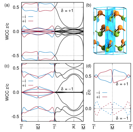
To corroborate the parity analysis, the hybrid Wannier charge centers (WCCs) are computed for the two dimerized states in the hexagonal structure having six Bi atoms (18 valence electrons) as shown in Fig. 4. Because of the inversion and time-reversal symmetries, the WCCs are mapped to symmetric copies as and , respectively. For , there are two WCCs crossing the cell boundary at () which is equal to the negative parity difference, (). Similarly, for , four (zero) WCCs cross the cell boundary at (), which also agrees well with the difference of negative parity states. The factor 2 from the spin degeneracy can be decomposed by grouping the WCCs based on the mirror eigenvalues on the - plane (see Fig.4). The WCCs with mirror eigenvalues and are denoted by blue and red lines, respectively. It is clearly seen that the number of boundary-crossing WCCs in each subspace is reduced by half. For example, a single blue line passes the boundary in Fig. 4(a). It agrees well with the mirror-symmetry-classified parity states in Table 1 where the negative parity states are divided in half () as well as their difference. Note that the number of negative parity states only provides an upper limit on the number of WCCs crossing the boundary, with the exact number of crossings being determined by the symmetry protection. Alexandradinata et al. (2014) The net Wannier center is shown in Fig. 4(d), where the half polarization of the Zak phase is clearly seen at the two TRIM, consistent with the parity results.
III Antiphase Domain Walls in Bi
The corresponding boundary states of the Zak phase can be realized on the (111) surface by appropriate choice of the surface termination that is usually hard to control. Fortunately, Bi is found to exhibit the Zak phase on the low-cleavage-energy surface. In general, however, the surface with Zak phase is susceptible to reconstruction and contamination. Aihara et al. (2020) Thus, instead of the bare surface, we consider antiphase DWs across which the sign of dimerization is reversed, , as shown in Fig. 5 and Fig. 7. The Bi (111) DWs, hosting the Zak phase, is indeed the 3D analogue of the 1D SSH model. The DW is tolerant to chemical contamination and can easily be found in a system exhibiting charge density wave.
In order to study the DW state without the interference from the neighbor DW, we use the interface Green’s function method Sancho et al. (1985); Ozaki et al. (2010) where the central DW structure is sandwiched between two semi-infinite pristine Bi with opposite dimerizations, as is shown in Fig. 5(b,c) for the (111) DW and Fig. 7(c,d) for the (11) DW. The construction of the Hamiltonian matrices is described in Appendix B. Throughout the remaining manuscript, the tilde () and bar () symbols over the -point labels denote TRIM points on the (111) and (11) DW BZ, respectively.
III.1 Non-trivial (111) Domain Wall


DW localized states – We have considered two types of (111) DWs shown in Fig. 5(b,c). In type-I DW (DW) the semi-infinite regions below (above) the DW has () dimerization. The central DW region has an inversion center, denoted by the horizontal black arrow, located on an atomic layer which is weakly bonded with its neighboring atomic layers along the stacking direction. In type-II DW (DW), the sign of dimerization is opposite and the central layer has strong bondings in both directions. The DW and DW correspond to the two types of DWs of the SSH model shown in Fig. 5(a),
The calculated DW spectral function is shown in Fig. 6(a,b) where the DW localized states (yellow lines) emerge inside the DW-projected bulk states (blue shade). Since inversion symmetry is preserved at the DW, all bands including the DW-localized yellow bands are doubly degenerate. Note that, regarding the interface band degeneracy, the DW localized states resemble Fig. 2(d) instead of Fig. 2(e) even with strong SOC. This is due to the inversion symmetry at the DW in a sharp contrast to the bare surface where the inversion symmetry is always broken. The Zak phase at and points induces an odd number of bands inside the bandgap that guarantees at least one band to be pinned at the Fermi level as long as the chiral symmetry persists. We find three DW localized states which are buried in the bulk bands at . At , however, the second band in the middle among them appears inside the bandgap indicating adequate chiral symmetry at the point compared to . 111 Our tight-binding parameters are tuned to open an insulating gap at, for example, , that is otherwise closed due to the overlap of electron and hole pockets (refers to Appendix A for details). The buried DW localized state, therefore, does not worsen the topological property of the DW. As discussed in Sec. I, the Zak phase corresponds to half polarization resulting in modulo surface charge per surface unit cell and half-filled in-gap state Aihara et al. (2020) (i.e., one electron per Kramers’ pair Zhang et al. (2013)). Integration of the spectral function at indeed confirms the half-filling of the in-gap state in both types of DWs. The DW localized band, marked with asterisk in Fig. 6, which emerges from the non-trivial state at is half-filled and hence metallic.
The number of DW-localized states can also be interpreted as the number of bonds truncated at the DW. On the (111) surface, a single Bi ion per unit cell is exposed with three bonds, consistent with the number of in-gap states. The number of bonds truncated at the DW is then determined by considering the Wannier function center, which is related to the Zak phase (see Eqs. 1 and 2). It is noteworthy that, for general systems with complicated terminations and reduced symmetries, a Green’s function approach can rigorously predict the number of surface or interface in-gap states Rhim et al. (2018) without suffering from the ion-truncating termination Hirayama et al. (2018) or lack of inversion symmetry. The metallic origin of the DW can be simply understood from its construction involving the intercalation of a monolayer in pristine bulk Bi, which in turn introduces three doubly degenerate bands near the Fermi level, where the second band is half filled since the number of available electrons is three.
The emergence of 2D Dirac cones at points in both DWs is unexpected and the crossing point is found to be lifted upon breaking the DW inversion symmetry. One way to break the inversion symmetry is to vertically translate the monolayer of DW. The translation eventually leads to a structure, equivalent to the DW, having a Bi tri-layer that recovers the inversion symmetry. Therefore, although the two DW structures [Fig. 5(b,c)] represent the 3D analogue of the SSH model, there is a general (111) DW structure without the DW inversion symmetry that will be referred to as type-III DW, DW (see Appendix B for the DW Hamiltonian). Figure 6(c) shows the calculated band structure of DW where the breakdown of inversion symmetry lifts the two-fold degeneracy of DW localized bands at generic points except at the surface TRIM. One significant difference of DW compared to the type-I and type-II DWs, is the splitting of the Dirac crossing at , which in turn forms three separate bands, indicating that the Dirac cone is related to the DW inversion symmetry rather than the Zak phase.

III.2 Trivial (11) Domain Wall
DW structure – In this section we consider two types of () DWs as shown in Fig. 7(c,d) where the dimerization direction lies on the DW plane. Thus, the () DWs can not be directly compared with the SSH model, in contrast to the (111) DW where its dimerization direction is normal to the DW plane that is a natural extension of the 1D SSH model (Fig. 1). Nevertheless, this raises the question of the emergence of () DW localized states and their topological nature. In both DW types, the central DW region is sandwiched between two semi-infinite pristine regions with opposite dimerization, involving a rigid shift of the right semi-infinite region relative to the left along the direction by , or vice versa. Detailed symmetries of the two DWs and consequent degeneracies of the band structure are further discussed in Appendix C.

DW Parity – Figure 3(c) shows the bulk and (11) interface BZs, where the bulk TRIM points are projected on the following interface TRIM points,
| (11) |
The parity flip induced by the dimerization reversal occurs at both the and points which are projected on the and points of the (11) interface BZ. Since the difference in the number of parity flips (Table 1) between the two dimerized domains is zero at and and four at and , the DW-projected Zak phases of both domains are the same, indicating the trivial topology of the DW states for both types of (11) DWs, unless certain crystal symmetry separates each band inversion. Since the mirror plane in Fig. 7(b) is common in both domains and the DWs one can group the parity states according to the mirror eigenvalues. Fig. 7(a) displays the hybrid WCCs labeled by the mirror-symmetry eigenvalues on and , which shows no evidence for non-trivial DW state.
DW localized states and symmetry – The band structures of the DW and DW are shown in Fig. 8, where eight of spin-degenerate DW-localized bands (yellow lines) appear inside the DW-projected bulk states (blue shade). The number of DW localized bands is related to the number of truncated bonds on the () plane which are eight in both DWs (see red planes in Fig. 7(c,d)). The fact that the number of in-gap states is even is consistent with the trivial Zak phase determined from the product of parity eigenvalues. Because of the complicated band dispersion and crossings of the DW localized states, we focus only on the high symmetry line on which the DW localized states are approximately four-fold degenerate. We find no specific crystal symmetry protecting such degeneracy. Nevertheless, an effective symmetry can be defined which can give rise to such degeneracy in the thick DW limit (Appendix C).
III.3 Arbitrary DW orientation
So far, we have considered Bi antiphase DW as a 3D analog of the SSH model with DW orientation either perpendicular or parallel to the dimerization direction. For the (111) DW, the projected parity flips across the DW inducing the Zak phase while the Zak phase is for the (11) DW. In order to predict the general behavior of the Zak phase for different DW orientations, we consider the possible ways of projecting the bulk TRIM points on various DW planes. For a surface or DW plane with Miller indices , the surface/interface normal vector is given by,
| (12) |
where the bi’s are reciprocal lattice vectors and the have no common factor. A pair of bulk TRIM points projected at the same point of the surface/interface BZ are always separated by , that is given by,
| (13) | |||||
| (14) |
where selects one TRIM point out of the eight and is an appropriate reciprocal lattice translation. The pair of TRIM points satisfy the following relation,
| (15) |
This demonstrates that the and are identical if the Miller index is even, otherwise they differ by one if is odd. Using this relation, one can enumerate all possible pairs of TRIM points which overlap on the projected 2D BZ of an arbitrary surface or DW, which are listed in Table 2. The (111) and (11) DWs correspond to (o,o,o) and (o,o,e) indices, respectively. The parity sign flip of Bi induced by dimerization reversal occurs at , and points in this notation. The antiphase DWs with Miller indices (e,e,o), (e,o,e), and (o,e,e) are expected to have parity sign flip across the DW giving rise to DW-localized states similar to the (111) DW or the SSH model. The remaining (e,o,o) and (o,e,o) DWs are expected to be trivial similar to the (11) DW. It is important to emphasize that since Table 2 is valid for arbitrary reciprocal lattice vectors, , it can be applied to a general centrosymmetric system. The only information required to predict a non-trivial DW orientation is to determine which TRIM point flips its parity product across the DW. It is even easier for bare surfaces, where the parity eigenvalues of the ground state are enough to predict a non-trivial surface orientation.
|
|
|||||||||||||||||||||||||||||||||||||||
III.4 Experimental Realization of Dimerization Reversal via Optical Pumping
There are two plausible experimental approaches to realize Bi antiphase DWs. The first approach is to search for dislocation defects in a Bi single crystal. For example, the (11) DW would appear on the (111) surface as a half step edge (step height of Bi monolayer, ) in scanning tunneling microscopy measurements. The second approach is to induce local dimerization reversal in pristine Bi using intense femtosecond laser-pump excitations, which have shown the reduction of the equilibrium displacement () of Bi, referred to as “ultrafast bond softening”. Fritz et al. (2007) More specifically, the laser-pump promotes valence electron into the conduction band and softens the Bi bond that agrees well with complementary density functional theory calculations. Fritz et al. (2007) The calculations also predict a transient structural transition to undimerized state () upon excitation of 2.5% of valence electrons. The energy barrier between the two dimerized ground states was found to decrease with increasing charge excitations, thus supporting the plausibility of dimerization reversal by excitations. Indeed, experiments confirmed that excitations higher than 2% lead to an irreversible “damage” to the samples suggesting that a permanent dimerization reversal may be achieved via the laser-pump excitations. Fritz et al. (2007)
IV Conclusion
We propose that the -phase of bulk Bi is a 3D manifestation of the SSH model. We demonstrate that while the HOTI and CTI phases of bulk Bi remain invariant under dimerization sign reversal, the Zak phase undergoes a transition from to 0. The (111) antiphase DW is found to host metallic DW bands, which are topologically protected due to the difference in polarization between the two oppositely dimerized domains (i.e., Zak phase), which is the 3D analogue of the SSH model. Although the (11) DW has no such polarization difference, the DW localized states exhibit interesting behavior related to an effective symmetry that reveals itself in thicker DWs.
To the best of our knowledge, this result is the first demonstration of the non-trivial Zak phase in 3D antiphase DWs. Unlike the bare surface being vulnerable to doping, contamination, or reconstruction, antiphase DWs offer a relatively stable platform for the manifestation of a non-trivial Zak phase. Furthermore, the common presence of DWs in charge-density-wave states offers a novel venue for investigating the potential of the non-trivial Zak phase.
V Methodology
The tight-binding parameters are extracted from the Wannier Hamiltonian obtained by using VASP-Wannier90 interface.Kresse and Furthmüller (1996a, b); Mostofi et al. (2014) The pseudopotentials are of the projector-augmented-wave type as implemented in VASP,Blöchl (1994); Kresse and Joubert (1999) with valence configurations 66 for Bi. The exchange-correlation functional is described by the Perdew-Burke-Ernzerhof generalized gradient approximation (PBE). Perdew et al. (1996) The plane-wave cut-off energy is set to eV and the Brillouin zone sampling grid is 12 12 12. The structure is relaxed with a constraint of being FCC for an insulating band gap. The twelve strongest hopping terms are then used in the calculation together with atomic spin-orbit coupling for the orbitals. The spectral density of DW-localized states is calculated using the interface Green’s function method Sancho et al. (1985); Ozaki et al. (2010) where two semi-infinite surface Green’s functions are first calculated for the two dimerized phases and then combined with the central DW Hamiltonian.
Acknowledgements.
This work at CSUN is supported by the NSF-Partnership in Research and Education in Materials (PREM) Grant No. DMR-1205734. D.V. was supported by NSF Grant DMR-1954856.Appendix A Tight-binding parameters
Although Bi has finite direct band gap in the whole BZ, its indirect gap between and points is negative causing metallic band structure and difficulties in the analysis of topological properties. For instance, the projected bulk states (blue shade in Fig. 8) at the point on the (11) BZ, should be gapless due to the negative indirect gap. In order to suppress the complexity, we have constructed the tight-binding parameters in the fcc instead of the rhombohedral cell, which in turn opens up a gap, shown in Fig. 3(b), without affecting the topological properties such as parities at the TRIM points.
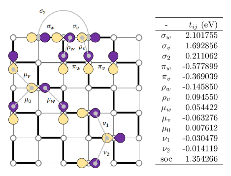
Figure 9 shows the selected twelve hopping terms in a dimerized cubic lattice and the amplitudes are listed in the inset table together with that of the atomic spin-orbit coupling. The , , and are the nearest-neighbor hoppings distinguished by the relative direction of the orbitals; the is the third nearest-neighbor -bond like hopping term; the terms vanish without dimerization because of the basis symmetry; the and terms are the second nearest-neighbor hoppings, and the terms do not change under dimerization reversal unless the direction of dimerization changes.
Appendix B Hamiltonian of the DW


The hopping terms with subscripts and modulate in the vicinity of the DW. The amplitude of the hopping terms is determined via linear interpolation of the two hopping terms by considering the distances of two basis from the DW plane. Namely,
| (16) | |||||
| (17) | |||||
| (18) |
where is the original hopping terms of Bi (Fig. 9) and is the mixing ratio depending on the weight factor representing the sign of dimerization as illustrated in Fig. 10 and 11. The DW and DW have 6 atomic layers along the stacking direction with one ion per layer. The DW has 14 ions and 7 vertical planes () in the cell while DW has 12 ions and 6 vertical planes. In this interpolation scheme, the weighting factors for the thinnest (11) DW are also listed with a subscript “thin” in the inset of Fig. 11. The results for thin DW case shown in Fig.12(b,d) are calculated using Hamiltonians generated with these weighting factors.
Appendix C Symmetry of DW

In type-I DW, DW, [Fig. 7(c)] where the Bi atoms lie on the DW plane, has inversion, mirror, and two-fold rotation symmetries. The two-fold rotation, around the [10] direction is denoted by the horizontal blue axis. On the other hand, type-II DW, DW, [Fig. 7(d)] intersects the bonds between atoms across the DW and has similar symmetries as DW except that the rotation is replaced by a screw symmetry involving a two-fold rotation around the [10] direction followed by a half a translation along the same axis. Namely,
| (19) | |||||
| (20) |
Because of the DW inversion symmetry, all bands are two-fold degenerate in the whole interface BZ. The high symmetry lines along ( and ) are invariant under the operation for the DW and the operation for the DW. In addition, the nonsymmorphic symmetry for DW guarantees a four-fold degeneracy at and where . Young and Kane (2015)
In Fig. 12(a,c) we display the zoom-in band structure of Fig. 8(a,b) on the high symmetry line for both types of DWs along with the corresponding -resolved spectral function (blue lines) at . The calculations of the spectral function for DW corroborate the emergence of single peaks at which are indeed four-fold degenerate. On the other hand, such a four-fold degeneracy is not protected by symmetry for DW, which, however, exhibits similar band folding at point, where the peaks in Fig. 12(a) have negligible splitting. Furthermore, the high symmetry line appears to be four fold degenerate in both types of DWs, which cannot not be explained by the crystal symmetries. This apparent four-fold degeneracy of the high symmetry line is found to be lifted as the DW thickness is reduced, as is clearly shown by the splitting of the peaks (denoted by red) in Fig. 12(b,d). This implies an effective symmetry which appears to be present only for thicker DWs.
It is worth to emphasize that the two types of DWs are distinguished only by the position of DW plane and the Hamiltonian difference between the two DWs becomes subtle with increasing DW thickness. Both Hamiltonians eventually acquire and symmetries in the thick DW limit. The two symmetries are combined to an effective symmetry of the DW which can be expressed as
| (21) |
consisting of a half translation operation that allows the BZ-unfolding, : [;] [;] and causes band degeneracy on the line. This emergent half translation symmetry naturally explains the apparent four-fold degeneracy (i) of the high symmetry line in both types of DWs, and (ii) at in DW.
References
- Heeger (2001) Alan J. Heeger, “Nobel lecture: Semiconducting and metallic polymers: The fourth generation of polymeric materials,” Rev. Mod. Phys. 73, 681–700 (2001).
- Su et al. (1979) W. P. Su, J. R. Schrieffer, and A. J. Heeger, “Solitons in polyacetylene,” Phys. Rev. Lett. 42, 1698–1701 (1979).
- Su et al. (1980) W. P. Su, J. R. Schrieffer, and A. J. Heeger, “Soliton excitations in polyacetylene,” Phys. Rev. B 22, 2099–2111 (1980).
- Zak (1989) J. Zak, “Berry’s phase for energy bands in solids,” Phys. Rev. Lett. 62, 2747–2750 (1989).
- Kitaev (2001) A Yu Kitaev, “Unpaired majorana fermions in quantum wires,” Physics-uspekhi 44, 131 (2001).
- Yu et al. (2020) Xiang-Long Yu, Liang Jiang, Ya-Min Quan, Tong Wu, Yuanzhen Chen, Liang-Jian Zou, and Jiansheng Wu, “Topological phase transitions, majorana modes, and quantum simulation of the su–schrieffer–heeger model with nearest-neighbor interactions,” Phys. Rev. B 101, 045422 (2020).
- Delplace et al. (2011) P. Delplace, D. Ullmo, and G. Montambaux, “Zak phase and the existence of edge states in graphene,” Phys. Rev. B 84, 195452 (2011).
- Liu and Wakabayashi (2017) Feng Liu and Katsunori Wakabayashi, “Novel topological phase with a zero berry curvature,” Phys. Rev. Lett. 118, 076803 (2017).
- Obana et al. (2019) Daichi Obana, Feng Liu, and Katsunori Wakabayashi, “Topological edge states in the su-schrieffer-heeger model,” Phys. Rev. B 100, 075437 (2019).
- Zhu et al. (2019) Linghua Zhu, Emil Prodan, and Keun Hyuk Ahn, “Flat energy bands within antiphase and twin boundaries and at open edges in topological materials,” Phys. Rev. B 99, 041117(R) (2019).
- Hirayama et al. (2018) Motoaki Hirayama, Satoru Matsuishi, Hideo Hosono, and Shuichi Murakami, “Electrides as a new platform of topological materials,” Phys. Rev. X 8, 031067 (2018).
- Aihara et al. (2020) Yusuke Aihara, Motoaki Hirayama, and Shuichi Murakami, “Anomalous dielectric response in insulators with the zak phase,” Phys. Rev. Research 2, 033224 (2020).
- Zhang et al. (2017) Yunwei Zhang, Hui Wang, Yanchao Wang, Lijun Zhang, and Yanming Ma, “Computer-assisted inverse design of inorganic electrides,” Phys. Rev. X 7, 011017 (2017).
- Ryu and Hatsugai (2002) Shinsei Ryu and Yasuhiro Hatsugai, “Topological origin of zero-energy edge states in particle-hole symmetric systems,” Phys. Rev. Lett. 89, 077002 (2002).
- Burkov et al. (2011) A. A. Burkov, M. D. Hook, and Leon Balents, “Topological nodal semimetals,” Phys. Rev. B 84, 235126 (2011).
- Fang et al. (2016) Chen Fang, Hongming Weng, Xi Dai, and Zhong Fang, “Topological nodal line semimetals,” Chinese Physics B 25, 117106 (2016).
- Vanderbilt and King-Smith (1993) David Vanderbilt and R. D. King-Smith, “Electric polarization as a bulk quantity and its relation to surface charge,” Phys. Rev. B 48, 4442–4455 (1993).
- Smeu et al. (2012) Manuel Smeu, Hong Guo, Wei Ji, and Robert A. Wolkow, “Electronic properties of si(111)- and related reconstructions: Density functional theory calculations,” Phys. Rev. B 85, 195315 (2012).
- Berry (1984) M. V. Berry, “Quantal phase factors accompanying adiabatic changes,” Proc. R. Soc. Lond. A 392, 45–57 (1984).
- King-Smith and Vanderbilt (1993) R. D. King-Smith and David Vanderbilt, “Theory of polarization of crystalline solids,” Phys. Rev. B 47, 1651–1654 (1993).
- Resta (1994) Raffaele Resta, “Macroscopic polarization in crystalline dielectrics: the geometric phase approach,” Rev. Mod. Phys. 66, 899–915 (1994).
- Rhim et al. (2017) Jun-Won Rhim, Jan Behrends, and Jens H. Bardarson, “Bulk-boundary correspondence from the intercellular zak phase,” Phys. Rev. B 95, 035421 (2017).
- Fu et al. (2007) Liang Fu, C. L. Kane, and E. J. Mele, “Topological insulators in three dimensions,” Phys. Rev. Lett. 98, 106803 (2007).
- Fu and Kane (2007) Liang Fu and C. L. Kane, “Topological insulators with inversion symmetry,” Phys. Rev. B 76, 045302 (2007).
- Fritz et al. (2007) D. M. Fritz, D. A. Reis, B. Adams, R. A. Akre, J. Arthur, C. Blome, P. H. Bucksbaum, A. L. Cavalieri, S. Engemann, S. Fahy, R. W. Falcone, P. H. Fuoss, K. J. Gaffney, M. J. George, J. Hajdu, M. P. Hertlein, P. B. Hillyard, M. Horn von Hoegen, M. Kammler, J. Kaspar, R. Kienberger, P. Krejcik, S. H. Lee, A. M. Lindenberg, B. McFarland, D. Meyer, T. Montagne, Éamonn D. Murray, A. J. Nelson, M. Nicoul, R. Pahl, J. Rudati, H. Schlarb, D. P. Siddons, K. Sokolowski-Tinten, Th. Tschentscher, D. von der Linde, and J. B. Hastings, “Ultrafast bond softening in bismuth: Mapping a solid’s interatomic potential with x-rays,” Science 315, 633–636 (2007), https://www.science.org/doi/pdf/10.1126/science.1135009 .
- Schindler et al. (2018) Frank Schindler, Zhijun Wang, Maia G. Vergniory, Ashley M. Cook, Anil Murani, Shamashis Sengupta, Alik Yu. Kasumov, Richard Deblock, Sangjun Jeon, Ilya Drozdov, Hélène Bouchiat, Sophie Guéron, Ali Yazdani, B. Andrei Bernevig, and Titus Neupert, “Higher-order topology in bismuth,” Nature Physics 14, 918–924 (2018).
- Hsu et al. (2019) Chuang-Han Hsu, Xiaoting Zhou, Tay-Rong Chang, Qiong Ma, Nuh Gedik, Arun Bansil, Su-Yang Xu, Hsin Lin, and Liang Fu, “Topology on a new facet of bismuth,” Proceedings of the National Academy of Sciences 116, 13255–13259 (2019), https://www.pnas.org/doi/pdf/10.1073/pnas.1900527116 .
- Alexandradinata et al. (2014) A. Alexandradinata, Xi Dai, and B. Andrei Bernevig, “Wilson-loop characterization of inversion-symmetric topological insulators,” Phys. Rev. B 89, 155114 (2014).
- Sancho et al. (1985) M P Lopez Sancho, J M Lopez Sancho, J M L Sancho, and J Rubio, “Highly convergent schemes for the calculation of bulk and surface green functions,” Journal of Physics F: Metal Physics 15, 851–858 (1985).
- Ozaki et al. (2010) Taisuke Ozaki, Kengo Nishio, and Hiori Kino, “Efficient implementation of the nonequilibrium green function method for electronic transport calculations,” Phys. Rev. B 81, 035116 (2010).
- Note (1) Our tight-binding parameters are tuned to open an insulating gap at, for example, , that is otherwise closed due to the overlap of electron and hole pockets (refers to Appendix A for details). The buried DW localized state, therefore, does not worsen the topological property of the DW.
- Zhang et al. (2013) Fan Zhang, C. L. Kane, and E. J. Mele, “Time-reversal-invariant topological superconductivity and majorana kramers pairs,” Phys. Rev. Lett. 111, 056402 (2013).
- Rhim et al. (2018) Jun-Won Rhim, Jens H. Bardarson, and Robert-Jan Slager, “Unified bulk-boundary correspondence for band insulators,” Phys. Rev. B 97, 115143 (2018).
- Kresse and Furthmüller (1996a) G. Kresse and J. Furthmüller, “Efficient iterative schemes for ab initio total-energy calculations using a plane-wave basis set,” Phys. Rev. B 54, 11169–11186 (1996a).
- Kresse and Furthmüller (1996b) G. Kresse and J. Furthmüller, “Efficiency of ab-initio total energy calculations for metals and semiconductors using a plane-wave basis set,” Computational Materials Science 6, 15 – 50 (1996b).
- Mostofi et al. (2014) Arash A. Mostofi, Jonathan R. Yates, Giovanni Pizzi, Young-Su Lee, Ivo Souza, David Vanderbilt, and Nicola Marzari, “An updated version of wannier90: A tool for obtaining maximally-localised wannier functions,” Comput. Phys. Commun. 185, 2309 – 2310 (2014).
- Blöchl (1994) P. E. Blöchl, “Projector augmented-wave method,” Phys. Rev. B 50, 17953–17979 (1994).
- Kresse and Joubert (1999) G. Kresse and D. Joubert, “From ultrasoft pseudopotentials to the projector augmented-wave method,” Phys. Rev. B 59, 1758–1775 (1999).
- Perdew et al. (1996) John P. Perdew, Kieron Burke, and Matthias Ernzerhof, “Generalized gradient approximation made simple,” Phys. Rev. Lett. 77, 3865–3868 (1996).
- Young and Kane (2015) Steve M. Young and Charles L. Kane, “Dirac semimetals in two dimensions,” Phys. Rev. Lett. 115, 126803 (2015).