Atomistic modelling and characterizaion of light sources based on small-amplitude short-period periodically bent crystals
Abstract
The feasibility of gamma-ray light sources based on the channeling phenomenon of ultrarelativistic electrons and positrons in oriented crystals that are periodically bent with Small Amplitude and Short Period (SASP) is demonstrated by means of rigorous numerical modelling that accounts for the interaction of a projectile with all atoms of the crystalline environment. Numerical data on the spectral distribution, brilliance, number of photons and power of radiation emitted by 10 GeV electron and positron beams passing through diamond, silicon and germanium crystals are presented and analyzed. The case studies presented in the paper refer to the FACET-II beams available at the SLAC facility. It is shown that the SASP bending gives rise to the radiation enhancement in the GeV photon energy range where the peak brilliance of radiation can be as high as on the photons/s/mrad2/mm2/0.1 % BW. The parameters of radiation can be tuned by varying the amplitude and period of bending.
1 Introduction
Intensive gamma-ray radiation can be generated by exposing oriented crystals (linear, bent, periodically bent) to ultrarelativistic beams of electrons and positrons. Such systems can be considered as novel Crystal-based Light Sources (CLS) that operate in the domain where technologies based on the magnetic field become incapable [1]. In exemplary case studies presented in Refs. [2, 3] the brilliance of radiation emitted in a diamond-based Crystalline Undulator (CU) by a 10 GeV positron beam available at present at the SLAC National Accelerator Laboratory [4] has been calculated. It is shown in the photon energy range above MeV, which is inaccessible to conventional synchrotrons, undulators and XFELs, the CLS brilliance exceeds that of laser-Compton scattering light sources [7] and can be higher than predicted in the Gamma Factory proposal to CERN [5, 6].
In this paper we demonstrate that the values of peak brilliance of radiation as high as photons/s/mrad2/mm2/0.1 % BW can be achieved in a much higher photon energy range, GeV, by propagating the FACET-II electron and positron beams [4] through linear and periodically bent oriented crystals of diamond, silicon and germanium.
In recent years significant efforts of the research and technological communities have been devoted to design and practical realization of novel gamma-ray CLSs [1, 3]. Manufacturing of CLSs is a subject of the current European Horizon-2020 project N-LIGHT [8] and Horizon-EIC-Pathfinder-2021 project TECHNO-CLS [9]. Construction of a CLS is a challenging technological task, which combines development of technologies for crystal samples preparation (engaging material science, solid state physics, nanotechnology) along with a detailed experimental programme (for CLS characterization, design and manipulation of particle beams, experimental characterization of the radiation) as well as theoretical analysis and advanced computational modelling for the visualisation and characterisation of CLSs.
When developed, CLSs will have many applications in basic sciences, technology and medicine. The potential applications include nuclear medicine, production of rare isotopes, photo-induced nuclear reactions, non-destructive imaging of complex molecular systems with the resolution allowing detection of the positions of the nuclei and gamma-ray material diagnostics.
Several schemes for short-wavelengths LS alternative to CLSs and not based on the magnets have been implemented of proposed. To be mentioned is the scheme based on the Compton scattering process of a low-energy laser photon from an ultra-relativistic electron. Being backscattered the photon acquires energy increase proportional to the squared Lorentz factor of the electron. This method has been used for producing gamma-rays in the energy range keV – MeV [10, 7, 11]. The Compton scattering of a laser photon is also possible from an ionic electron that moves being bound to a nucleus. This phenomenon is behind the Gamma Factory proposal for CERN [5, 6] that implies using a beam of ultra-relativistic ions in the backscattering process. The intensity of an ion-beam-driven light source in the photon energy range MeV is expected to be several orders of magnitude higher than that achievable with Compton gamma-ray sources driven by an electron beam. In Ref. [12] a scheme for high-brilliance -rays with photon energies up to GeV by means of a two-stage laser-wakefield accelerator driven by a single multi-petawatt laser pulse has been proposed. In a recent study [13] a possibility of radiation generation at the wavelengths down to a picometer range (up to the MeV range in the photon energy) by means of a proposed future lepton-hadron Large Hadron electron Collider at CERN is discussed.
The concept of a CLS relies on the channeling phenomenon which stays for a large distance penetration of a charged projectile that move along a crystallographic plane (planar channeling ) or axis (axial channeling) experiencing collective action of the electrostatic fields of the lattice atoms [15]. An average distance covered by a channeling particle before leaving this mode of motion due to uncorrelated collisions is termed a dechanneling length, . This quantity depends on the crystal type and its orientation, the energy and charge of the projectile. To mitigate a destructive impact of dechanneling on the channeling motion as well on the emission of the associated radiation the crystal thickness along the incident beam must be chosen as .
A number of theoretical and experimental studies of the channeling phenomenon in linear crystals have been carried out [16]. A channeling particle emits intensive channeling radiation (ChR)[17], the characteristic energy of which scales with the particle beam energy as and thus can be varied by changing . For example, electrons of moderate energies, MeV, channeled in a linear crystal generate ChR of energy keV [18]. High-quality electron beams of tunable energies within the tens of MeV range are available at many facilities. Hence, it has become possible to consider ChR from linear crystals as a new X-ray light source [18].
ChR in the gamma-range can be emitted by electron (or positron) beams of higher energies, . As a rule, modern accelerator facilities operate at a fixed value of (or, at several fixed values) [4, 19, 20]. In this case, to make CLSs tunable with respect to the energy of radiation one can consider using different linear crystals111Oriented diamond, silicon and germanium crystals have been used in channeling experiments with beams of ultra-relativistic leptons [16, 21, 22, 23, 24, 27, 26, 25]. or/and other than linear geometries of crystalline samples. From this viewpoint, the use of bent and, especially, periodically bent crystals can become proper targets as they provide tunable emission in the gamma-ray range [28, 1].
As formulated originally [29, 30, 31], the concept of a crystalline undulator (CU) implies that a charged projectile channels following periodically bent planes of the crystal. The amplitude of periodic bending is assumed to be larger that the interplanar distance but much less than the bending period . Then, provided several conditions are fulfilled, the projectile is steered along the bent plane experiencing, simultaneously, the channeling oscillations. The inequalities ensure that frequencies of the undulator modulation are much smaller than the channeling oscillations frequencies. As a result, in the spectral distribution of radiation the peaks of CU radiation (CUR) appear at energies well below those typical for ChR [29, 30, 31]. By varying , and the crystal length one can tune the peak positions and intensities [28]. Initial estimates [3] and more accurate results of rigorous numerical simulations [2] have demonstrated that the brilliance of CLS based on the FACET-II positron beam channeling in periodically bent diamond crystals in the photon energy range MeV can be as high photons/s/mrad2/mm2/0.1 % BW.
Another regime of periodic bending, termed Small-Amplitude Short-Period (SASP) [32], implies the bending with and shorter than the period of channeling oscillations. In this case the trajectory of a channeling particle does not follow the profile of bent planes but experiences a jitter-type modulations resulting from the short-period bending. These modulations lead to the radiation emission at the energies well above the peaks of ChR [32, 33, 34, 35].
Periodically bent crystals with both types of bending can be manufactured by means of modern technologies, a review of which can be found in Refs. [3, 1]. In particular, the SASP bending can be achieved by varying the fraction of the germanium atoms in the process of the epitaxial growth Si1-xGex superlattice [36, 37] The SASP crystals can also be produce by doping with boron or nitrogen in the process of synthesising a diamond superlattice [41]. By means of the former method sets of SASP periodically bent Si1-xGex superlattices have been produced and used in channeling experiments at the MAinz MIkrotron (MAMI) and the SLAC facilities [38, 39, 40].
In this paper we present a comprehensive comparative analysis of the channeling properties and the radiation by 10 GeV electrons and positrons passing through linear and SASP bent diamond, silicon and germanium crystals. When analyzing the radiation emitted the focus is made on the quantities that characterize the system ’beam of particles and a crystal’ as a potential crystal-based light source. Apart from the spectral distribution of radiation, the list of such quantities includes: brilliance, number of the photons per unit time and power of radiation. All these quantities are dependent on the beam current, ; the brilliance, in addition, is strongly sensitive to the beam sizes and divergencies in the transverse direction. Therefore, the case studies presented in Section 2 refer to the FACET-II electron and positron beams at the SLAC facility [4], the bunches of which are characterized by small transverse emittance and high peak current.
Numerical simulations of the channeling and radiation processes beyond the frequently used continuous potential framework has been carried out by means of the multi-purpose computer package MBN Explorer [42, 43, 44] and a supplementary special multitask software toolkit MBN Studio [45]. The MBN Explorer package was originally developed as a universal computer program for multiscale simulations of structure and dynamics ofcomplex Meso-Bio-Nano (MBN) systems. MBN Studio is a powerful multi-task toolkit used to set up and start MBN Explorer calculations, monitor their progress, examine calculation results, visualize inputs and outputs, and analyze specific characteristics determined by the output of simulations A special module of MBN Explorer allows one to simulate the motion of relativistic projectiles along with dynamical simulation of the environment [43]. The uniqueness of the computation algorithm is that it accounts for the interaction of projectiles with all atoms of the environment thus making it free of simplifying model assumptions. In addition, a variety of interatomic potentials implemented facilitates rigorous simulations of various media, a crystalline one in particular. Overview of the results on channeling and radiation of charged particles in oriented linear, bent and periodically bent crystals simulated by means of MBN Explorer and MBN Studio can be found in [3, 35, 28, 44].
2 Results and discussion
2.1 Parameters used in the simulations
Trajectories of 10 GeV electrons and positrons have been simulated in microns thick oriented diamond(110), silicon(110) and germanium(110) crystals. The simulations have been performed for the linear crystals as well as for the SASP periodically bent crystals. In the latter case the harmonic profile of the periodic bending of the (110) planes has been considered with the coordinate measured along the non-deformed () plane. The direction of the -axis was chosen well away from crystallographic axes to avoid the axial channeling regime. The -axis was chosen along the axial direction. The bending amplitude was considered within the range Å, the values of the bending period were and 600 microns. We note that these values of and are close to those used in the channeling experiments with the SASP crystals [38, 39, 40].
In the course of simulations the positions atoms in either linear or periodically bent crystalline structure was generated with account for their random displacement from the nodes due to thermal vibrations at temperature K. For each atom the displacement from the node was generated using the normal distribution with the root-mean-square amplitude of the thermal vibrations equal to 0.04, 0.075 and 0.085 Å [46]. More details on the simulation procedure as well on the formalism behind it can be found in Ref. [43] and in the review paper [35].
For each trajectory simulated the initial conditions at the crystal entrance (i.e. and coordinates and the corresponding velocities) were generated assuming the Gaussian distributions of the beam particles in the transverse coordinates and velocities. The root mean square (rms) beam sizes and angular divergences used in the simulations are presented in Table 1 along with other parameters that correspond to the GeV (the relativistic Lorentz factor is ) electron and positron beams. The data on the beam size, normalized rms emittance , and peak current are taken from Table 4.7 in Technical Design Report for the FACET-II beam at the SLAC facility, Ref. [4]. The divergencies indicated in the table were calculated from the and values.
| (m-rad) | (m-rad) | (m) | (m) | (rad) | (rad) | (kA) | |
| Electron | 4.0 | 3.2 | 6.8 | 16.3 | 30 | 10 | 64 |
| Positron | 10 | 12 | 17 | 61 | 30 | 10 | 5.8 |
As mentioned, in the simulations the -axis was chosen perpendicular to the planar direction. This choice ensures that the biggest fraction of a Gaussian beam with angular divergence rad enters the crystal having the incident angle with respect the plane much less that Lindhard’s critical angle , i.e. such particles can be accepted in the channeling mode at the entrance. This fraction can be estimated as . Using the vaues eV for the interplanar potential depth in (110) planar channels in the diamond, silicon and germanium one finds, respectively, and 88 rad that exceeds by large factors the divergence , hence in all cases. The beams divergence rad along the direction is smaller than the natural emission angle rad. As a result, one can expect that big fraction of radiation emitted by the channeling particles will be collected within the cone centered along the incident beam.
2.2 Statistical properties of channeling
Due to the randomization of the conditions at the crystal entrance as well as of the positions of the lattice atoms that are subject to thermal fluctuations, each trajectory simulated corresponds to a unique crystalline environment. Statistical independence of the trajectories allows one to quantify the channeling process in terms of several functional dependencies which appear as a result of statistical analysis of the trajectories.
In the course of passing through an oriented crystal a charged projectile can experience different types of motion including the channeling and overbarrier motion. The transition from the channeling to the overbarrier motions, - the dechanneling process, as well as the opposite transition, - the rechanneling process, occur due to uncorrelated collisions of the projectile with the crystal atoms. To quantify these processes the following two dependencies, termed channeling fractions, can be considered [43, 47]. One of these is defined as where is the number of accepted particles, i.e. those which experience the channeling motion at the crystal entrance, . The numerator, , stands for the number of accepted particles that channel up to the distance where they dechannel. To quantify the efficiency of the rechanneling process one can construct another fraction, with being the total number of particles which move in the channeling mode at distance .


The fraction is a decreasing function of the penetration distance due to gradual dechanneling of the accepted particles. At sufficiently large distances this fraction decreases following the exponential decay law, [48], where stands for the dechanneling length. In contrast, the fraction is a non-monotonous function: in the vicinity of the entrance point it increases due to the rechanneling of the non-accepted particles and at larger distances, as the beam becomes more divergent because of the multiple scattering and thus dechanneling rate exceeds the rechanneling one, it decreases. In the region and above this fraction can be be approximately written in terms of the error function where is the fitting parameter [35].
Figure 1 shows the dependencies (solid lines with symbols) and (solid lines without symbols) obtained from the simulated trajectories of electrons (upper row) and positrons (lower row) in linear diamond, silicon and germanium crystals. A striking difference in the behaviour of the two fractions as functions of the penetration distance is mostly pronounced for electrons (note different scale in the vertical axes in the graphs for electrons and positrons). Away from the entrance point the fraction follows approximately the exponential decay law, see red dashed lines without symbols. The values of the dechanneling lengths used to construct the fits are indicated in the caption. Red dashed lines with squares show the fits for with the fitting parameters as indicated in the caption. It is seen that this fraction decreases much slower than , which does not account for the rechanneling. At large distances . The crystal thickness m used in the simulations is order of magnitude smaller than the positron dechanneling lengths estimated from the dependencies . As a result, both fractions do not differ much even in the case of a higher- germanium crystal. On this scale of the fraction does not exhibit its asymptotic behaviour, therefore, no fitting curves are presented.
2.3 Spectral distribution of radiation
Spectral distribution (per particle) of the radiant energy emitted within the cone along the incident beam is evaluated numerically by means of the formula
| (1) |
Here, is the radiation frequency, is the solid angle corresponding to the emission angles and . The sum is carried out over all simulated trajectories of the total number (in the current simulations ). For each trajectory the spectral-angular distribution of the radiation is computed by numerical integration as described in detail in [43].
To compute the spectral distribution of radiation emitted the quasi-classical formalism [49] is used. It accounts for the quantum recoil that becomes important when the photon energies are no longer negligible compared to the energies of projectiles, . In Refs. [34, 35], it was demonstrated that photons of such energies are emitted by multi-GeV electrons and positrons passing through SASP periodically bent crystals.
The energy of the first harmonic of radiation due to the SASP modulations of the particle’s trajectory depends rather weakly on the bending amplitude [34] and can be estimated from the following relation [49]:
| (2) |
where is the peak position of the radiation if the quantum recoil is neglected. Table 2 presents the values of and calculated for GeV projectiles.
| 200 | 400 | 600 | |
|---|---|---|---|
| 4.75 | 2.375 | 1.58 | |
| 3.22 | 1.92 | 1.36 |
For the sake of reference let us estimate the photon energies that correspond to the peaks of the channeling radiation in linear crystals. This can be done applying the harmonic approximation for the interplanar potential (this model is adequate for positively charged projectiles):
| (3) |
where and stand for the interplanar potential well depth and the interplanar spacing. For the (110) planes in diamond, silicon and germanium crystals these parameters are as follows222The indicated values of correspond to the Moliére continuous potential calculated at the crystal temperature K, Ref. [35]: Å, eV. Using these values in Eq. (2) one finds that for all aforementioned crystals the peaks of ChR emitted by a 10 GeV positron is located at MeV i.e. order of magnitude lower than the photon energies due to the SASP bending.


To establish the ranges of bending amplitudes and periods that provide the largest values of the radiated energy, we have opted to study first radiation for comparatively thin, m, crystals. Figures 2-4 present the spectral distribution of radiation emitted within the cone rad by electrons (left column) and positrons (right column) incident along the (110) crystallographic planes in diamond, silicon and germanium crystals. In each figure three rows of graphs refer to different values of the bending period as indicated. In each graph the curves refer to the amplitudes as specified in the common legend located in the middle row graphs.
The spectra formed in the linear crystals, , (black solid-line curves) are dominated by the peaks of ChR. The peak intensity greatly exceeds the intensity of the incoherent bremsstrahlung radiation (its values are indicated in the caption) emitted by the projectiles in the corresponding amorphous media. In the case of positron channeling, the peaks exhibit some internal structure due to the emission in the first and the second harmonics of ChR. This feature is more pronounced for the germanium target where the two maxima are clearly seen whereas in the spectra for diamond and silicon the second harmonics reveals itself as a step-like structure on the right shoulder. The positions of the first-harmonic peaks correlate with the estimates presented above, see Eq. (3). For the electrons, the ChR peaks are broadened and less intensive as a result of strong anharmonicity of the channeling oscillations.
The radiation spectra produced in the SASP bent crystals () display two novel features. These are (i) lowering and, in the electron case, red-shifting of the ChR peaks [33], and (ii) emergence of additional peaks that are due to the short-period modulations of the projectile trajectories [32, 34].
Qualitative explanation of the changes in the ChR peaks is as follows.
In a linear crystal, due to thermal vibrations, the nuclei of atoms of a crystal plane are distributed within a layer of the width to , where is the rms amplitude of the vibrations. Using the Thomas-Fermi model one estimates the atomic radius as where is the nucleus charge and is the Bohr radius. Hence, in the linear crystal the density of atomic nuclei and electrons is concentrated primarily within the layer . In this region a channeling particle experiences frequent collisions with the atoms, which result in the dechanneling event. Hence, stable channeling motion, which leads to the intensive ChR, occurs if the particle’s trajectory (or most of it) is outside this regions. Positrons channel between two adjacent plains, therefore, this condition sets an upper bound on the amplitude of channeling oscillations, . In the case of electron channeling, which occurs in the vicinity of a plane, the amplitude’s value acquires the lower bound equal to . When the plane is subjected to the SASP bending with amplitude , the layer of the increased density becomes wider, . As a result, the number of channeling particles decreases and so does the intensity of ChR for the projectiles of both types. However, the mechanisms of the additional modification of the ChR peak are different for positively and for negatively charged projectiles. The SASP bending lowers the upper bound of for positrons making it equal to but for electrons the effect is the opposite: more favourable are channeling trajectories with the amplitudes larger than in the linear channel, . Due to nearly harmonic character of the positron channeling oscillations the decrease in leads to lowering the intensity of the ChR peak but does not affect its position. Strong anharmonicity of the electron channeling oscillations makes their frequency dependent on the amplitude. In particular, is a monotonously decreasing function of for the (110) planar channels in diamond, silicon and germanium crystals [28]. Taking into account that the photon energy is proportional to one concludes that the increase in leads to stronger suppression of the ChR in the region of higher photon energies. As a result, the ChR peaks become less intensive and red-shifted.
The second feature in the emission spectra presented in Fig. 2-4 is the peaks due to the SASP periodic bending. These peaks are located in the domain of higher photon energies and their positions agree well with the estimated values of indicated in Table 2. As it is seen from the figures, for both types projectiles and for all three crystals considered the peak intensity at a fixed value of the amplitude is inversely proportional to the bending period . For a given the peak intensity increases from zero at up to the maximum value at some amplitude and then decreases with further increase in [33]. For the case studies considered here the values were found to be equal to 0.3 Å for diamond and silicon, and to 0.5 Å for germanium.
In what follows we focus on the characteristics of radiation (spectral distribution, brilliance, power and number of photons) emitted in linear crystals and in the periodically bent crystals with amplitude Å and period nm.


Figures 5-7 compare the spectral distributions of radiation formed in linear (upper rows) and periodically bent (lower rows) oriented diamond, silicon and germanium crystals of different thickness ranging from 6 m up to 96 m. In each figure the left and right columns refer to the electron and positron channeling, respectively. All spectra correspond to the emission cone along the incident beam.
The following features of the spectra are to be noted.
In the linear crystals the (main) peak of ChR emitted by positrons is higher and narrower that the corresponding peak for electrons in a crystal of the same type and thickness. In the shorter crystals both of these features are due to different character (harmonic or anharmonic) of the channeling oscillations experienced by positively and negatively charged projectiles. As the crystal thickness increases, the intensity of ChR by electrons is additionally suppressed due to much higher dechanneling rate. The particles that leave the channeling mode of motion produce much less intensive radiation as compared to those that continue the channeling motion. The rechanneling process brings part of the particles back to the channeling mode mode, nevertheless, the fraction of channeling electrons decreases with the penetration distance much faster than that of the positrons, see Fig. 1. This effect is more pronounced for the high- crystal, germanium. As a result, for all crystals the emission spectra of positrons scale linearly with thickness in the whole interval of the values. For electrons, this is true only in the case of the low- target, diamond. For silicon and, especially, germanium, the linear dependence is seen over shorter intervals of .
Another feature seen in the positron spectra in both the linear and periodically bent crystals is the emergence of the peaks corresponding to higher harmonics of ChR. The peaks associated with the second harmonic are well pronounced in the spectra starting with m, in some cases (linear diamond, linear and periodically bent germanium) the emission in the third harmonic is also seen. To provide an explanation one recalls that channeling oscillations of positrons are nearly harmonic. This results in the emission of the undulator-type radiation. The width of the peak of the the harmonic of the undulator radiation as well as its natural emission cone decrease with the number of undulator periods: and (see, e.g., [50]). As a result, the larger is the more separated the harmonics become, especially if the radiation is collected within a (comparatively) narrow cone along the undulator axis. Applying these arguments to the positron spectra one concludes that as increases so does the number of periods of channeling oscillations. Hence, the emission in higher harmonics becomes more pronounced.333The smaller the emission cone is the larger number of the higher harmonic peaks are resolved in the ChR spectrum, see Section B.
The spectra presented in the lower graphs in Figs. 5-7 demonstrate the notable increase in the intensity in the photon energy range 0.8…1.4 GeV due to the SASP periodic bending. The position and the height of the SASP peaks are virtually not sensitive to the projectile’s charge but strongly depend on the crystal type and thickness.
To further characterize the emission produced in linear and periodically bent crystals we consider the largest value of the target thickness, m.
2.4 Brilliance of radiation
One of the quantities used to compare light sources of different nature is called brilliance, . It is defined in terms of the number of photons emitted by the particles of the beam within the interval in the solid angle (the emission cone is assumed to be small, ) per unit time interval, unit source area, unit solid angle and per a bandwidth (BW) [51]. To calculate brilliance of a photon source of a finite size it is necessary to know the beam current , beam sizes and angular divergence in the transverse directions as well as the divergence angle and the ’size’ of the photon beam.
Explicit expression for brilliance written in terms of the spectral distribution reads
| (4) |
Here stand for the total emittance of the photon source in the transverse directions
| (5) |
where and is the ’apparent’ source size taken in the diffraction limit [52] ( is the radiation wavelength).
Commonly, brilliance is measured in . To achieve this in Eq. (4) the current is measured in amperes, in millimeters, and in milliradians.
If one uses the peak value of the current, , then the corresponding quantity is called peak brilliance, .


Figures 8-10 show the peak brilliance of radiation emitted by the electron (left columns) and positron (right columns) beams channeling along the (110) planar direction in m thick linear (upper rows) and SASP bent (lower rows) diamond, silicon and germanium crystals. In each graph the curves correspond to different emission cones that measured in units of the natural cone as indicated in the common legend in each figure. The dependencies presented have been obtained from Eq. (4) with the total emittances (5) calculated using the values of and indicated in Table 1. The values and 5.8 kA were used for the electron and positron beams, therefore, the dependencies presented in the figures refer to the brilliance of radiation emitted by a single bunch of the beams.
The spectral distributions that have been used to calculate the brilliance are shown in Figs. 15-17 in Section B. It is seen that in contrast to , which is an increasing function of the emission cone for all values of , the peak brilliance can exhibit a non-monotonous behaviour due to the presence of the terms proportional to in the total emittance. The case studies presented by the figures demonstrate that by means of the FACET-II electron beam it is possible to achieve peak value photons/s/mrad2mm2/0.1 % BW for the channeling radiation in the linear diamond crystal in the photons energy range MeV and the value photons/s/mrad2mm2/0.1 % BW in the SASP bent diamond crystal for much higher photon energies, GeV. The peak brilliance achievable by means of the positron beam are noticeably smaller. This is despite the fact that the values of for positrons are either higher (in the vicinity of the channeling peak) or approximately equal to (for the peak due to the SASP bending) those for electrons, see Figs. 15-17. This is a direct consequence of the difference in the parameters of the two beams, namely, the factor , which enters the right-hand side of (4), is two orders of magnitude larger in the case of the electron beam.

Figure 11 compares the peak brilliance of radiation emitted by the FACET-II electron beam incident along the (110) directions at linear (left graph) and periodically bent (right graph) diamond, silicon and germanium crystals. The highest values of are achievable for the diamond target. In the linear crystal, the values of achievable in the photon energy range 100-400 MeV are compared to those predicted in Ref. [12] for a high-brilliant light source based on a two-stage laser-wakefield accelerator driven by a single multi-petawatt laser pulse. However, in the photon energy range about 1 GeV the SASE CLS peak brilliance is orders of magnitude higher than the quoted valus (see Figure 2 in the cited paper).
2.5 Power and number of photons
To characterize the radiation emitted by a beam of particles it is instructive to calculate, in addition to spectral distribution and brilliance, two other commonly used characteristics - the number of photons per unit time and the power of radiation emitted within the cone and the bandwidth . Both of these quantities are expressed in terms of spectral distribution and beam current . The corresponding relations are as follows:
| (6) | |||||
| (7) |

Using the peak current on the right-hand side of (6) one determines the instantaneous value of . Calculated for the FACET-II electron beam this quantity as a function of the photon energy is shown in Fig. 12 two panels of which refer to the linear (left) and periodically bent (right) (110) channels in m thick diamond, silicon and germanium crystals. The curves presented correspond to the bandwidth and to the natural emission cone .
It is instructive to compare the values obtained here with the number of photons per second predicted in the Gamma Factory (GF) proposal for CERN [5, 6], where a light source based on the resonant absorption of laser photons by ultra-relativistic ions has been elaborated. Within the GF proposal it is expected to achieve the average number of photons on the level of photons/s in the photon energy range 1-400 MeV. This value refers to the average beam current. To estimate the corresponding instantaneous value one multiplies by a factor , which is the ratio of the bunch spacing ( ns) to the bunch length ( ns) [1, 2]. The dashed line drawn in both graphs in Fig. 12 indicates the estimated instantaneous value of photons/s in the photon energy range specified above. To be noted is that the value of the FACET-II peak current correspond to a much shorter bunch (several picoseconds [4].
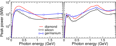
The peak power of radiation from the electron beam is presented in Fig. 13. It is seen that by means of the SASP bending it is possible to achieve the same values of the power as in the linear crystal but for the photons of much higher energy.
3 Conclusion
In this paper the method of all-atom molecular dynamics has been applied to simulate the channeling process and the radiation emission by 10 GeV electron and positron beams in oriented diamond, silicon and germanium crystals. The beams’ parameters (sizes, divergencies, peak currents) used in the simulations have been chosen to match the parameters of the FACET-II beams [4].
The exemplary case studies presented in the paper are focused on the comparison of the radiation emitted in the linear and in the Small-Amplitude Short-Period (SASP) periodically bent crystals. In the latter, in addition to the channeling radiation, the enhancement of the photon yield due to the short-period modulation of the particles’ trajectories appears in the GeV photon energy range that is well-above the energies of the channeling radiation. The characterization of the gamma-ray Crystal-based Light sources, carried out for all crystals considered and for both beams, includes calculation of spectral distribution of radiation, its instantaneous (peak) brilliance, number of photons per second and power. It is demonstrated that the values of peak brilliance and number of photons per second achievable in the SASP CLSs in the GeV energy range exceed those predicted for the alternative novel schemes of gamma-ray light sources [5, 12].
The bending period in a SASP crystal lies in the range of hundreds of nanometers. As a result, a large number of periods can be realized in crystals of a comparatively small thickness, starting from few tens of microns, that in many cases is less than the dechanneling length of electrons. This, in turn, allows for considering the SASP CLSs based on the channeling phenomenon of both positively and negatively charged projectiles.
By tuning the bending amplitude and period one can vary the spectral intensity of radiation and maximize its brilliance for given parameters of a beam and/or chosen type of a crystalline medium. This will allow one to make an optimal choice of the crystalline target and the parameters of the SASP bending to be used in a particular experimental environment or/and to tune the parameters of the emitted radiation matching them to the needs of a particular application.
Appendix A Spectral distribution within the Bethe-Heitler approximation
The approximation widely used to describe the bremsstrahlung (BrS) process of a relativistic charged projectile in the static field of an atomic (ionic) target is due to Bethe and Heitler [53] (with the corrections introduced later [54, 55, 56]).
For the sake of reference we present the explicit expression for the differential cross section of BrS emitted with the cone by an ultra-relativistic electron/positron in collision with a neutral atom treated within the Molière approximation [57]. Starting from Eq. (3.80) in Ref. [56] one derives [43]:
| (8) | |||||
Here is the fine structure constant, cm is the classical electron radius, , ( is the atomic number) and .
The term stands for the BrS cross section integrated over all emission angles (, hence ):
| (9) |
The rest part of the expression on the right-hand side of (8) is the correction due to limiting the emission cone.
The factor reads
| (10) |
where the function (with ) is the Coulomb correction to the first Born approximation worked out in Refs. [54, 55]. In the limit the term can be ignored.
To calculate the spectral distribution of radiated energy within the Bethe-Heitler (BH) approximation in an amorphous target of the thickness one multiplies Eq. (8) by the photon energy , by the volume density of the target atoms and by :
| (11) |
Figure 14 shows the BH spectra emitted within the cone by a 10 GeV projectile in amorphous “diamond” ( cm-3), silicon ( cm-3) and germanium ( cm-3) targets of thicknesses and m.

We note that the spectra presented in 14 are calculated using Eq. (8) in (11). This frammework does not take into account the angular spread of the beam particles due to the multiple scattering and also it implies an ideally collimated beam (zero divergence). In other words, the use of Eq. (11) is applicable if where stands for the beam divergence and is the rms angle of multiple scattering. To estimate one can use Eq. (33.15) from Ref. [19]:
| (12) |
where is the radiation length, i.e. the average distance over which an ultrarelativistic particle on passing through a medium looses its energy due to the radiation emission [58]. Utilizing Eq. (33.20) from Ref. [19]) one obtains the following values of for amorphous carbon, silicon and germanium: 12.2, 9.47 and 2.36 cm.
Applying (12) to a MeV electron/positron passage through amorphous carbon, silicon and germanium one obtains, respectively, rad for m and rad for m. Therefore, for lighter substances (diamond, silicon) the BH spectra calculated for rad, see Fig. 14, can be considered as reasonable estimates for all values indicated whereas for germanium the curves shown for and 96 m overestimate the realistic spectra.
Appendix B Simulated spectral distribution for different opening angles
In this Section we present radiation spectra calculated for different emission cones, . The spectra data have been used as the input data to calculate brilliance and power of the radiation as well as the number of photons per second emitted by the 10 GeV electron and positron FACET-II beams passing through linear and SASP periodically bent diamond, silicon and germanium crystals along the (110) planar direction.
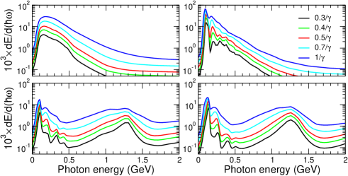
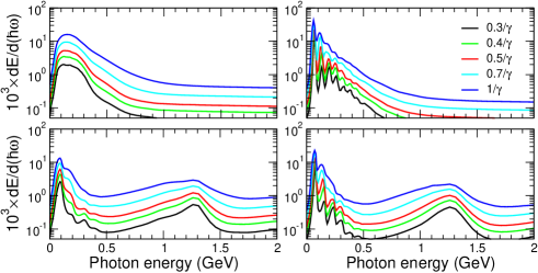

The spectral distributions shown in Figs. 15-17 all refer to the crystal thickness . In each figure the upper row correspond to the linear crystal and the lower row to the periodically bent crystal. The SASP bending amplitude and period are Å and nm. Left and right columns present the electron and positron spectra, respectively. The emission cones are indicated in the common legend being measured in the units of the natural emission cone .
Most of the features seen in the spectra presented are similar to those discussed in connection with Figs. 5-7. To be additionally noted is that, apart from the monotonous increase in the absolute value of with in the whole range of photon energies, the peaks due to ChR and the SASP-induced radiation become noticeably broader.
References
References
- [1] A. V. Korol and A. V. Solov’yov. Novel Light Sources beyond Free Electron Lasers, Springer Nature Switzerland AG, 2022.
- [2] G. B. Sushko, A. V. Korol and A. V. Solov’yov. Extremely brilliant crystal-based light sources, Europ. Phys. J. D (2022) (in press).
- [3] A. V. Korol and A. V. Solov’yov. Crystal-based intensive gamma-ray light sources. Europ. Phys. J. D 74, 201 (2020).
- [4] SLAC Site Office: Technical Design Report for the FACET-II Project at SLAC National Accelerator Laboratory. Report SLAC-R-1072, SLAC (2016).
- [5] M. Krasny. The Gamma Factory proposal for CERN. CERN Proc. 1, 249 (2018).
- [6] M. W. Krasny, A. Martens, Y. Dutheil. Gamma factory proof-of-principle experiment: Letter of intent. CERN-SPSC-2019-031/SPSC-I-253, 25/09/2019 (http://cds.cern.ch/record/2690736/files/SPSC-I-253.pdf).
- [7] C. R. Howell, M. W. Ahmed, A. Afanasev, D. Alesini, J. R. M. Annand, et al. International Workshop on Next Generation Gamma-Ray Source. Phys. G: Nucl. Part. Phys. 49, 010502 (2022).
- [8] http://www.mbnresearch.com/N-Light/main
- [9] http://www.mbnresearch.com/TECHNO-CLS/Main
- [10] Norihiro Sei, Hiroshi Ogawa, and QiKa Jia. Multiple-Collision Free-Electron Laser Compton Backscattering for a High-Yield Gamma-Ray Source. Appl. Sci. 10, 1418 (2020).
- [11] Y. K. Wu, N. A. Vinokurov, S. Mikhailov, J. Li, and V. Popov. High-Gain Lasing and Polarization Switch with a Distributed Optical-Klystron Free-Electron Laser. Phys. Rev. Lett. 96, 224801 (2006).
- [12] Xing-Long Zhu, Min Chen, Su-Ming Weng, Tong-Pu Yu, Wei-Min Wang, Feng He, Zheng-Ming Sheng, Paul McKenna, Dino A. Jaroszynski, and Jie Zhang. Extremely brilliant GeV -rays from a two-stage laser-plasma accelerator. Science Advances 6, eaaz7240 (2020).
- [13] Z. Nergiz, N. S. Mirian, A. Aksoy, D. Zhou, F. Zimmermann, and H. Aksakal. Bright Angstrom and picometer free electron laser based on the Large Hadron electron Collider energy recovery linac. Phys. Rev. Accel. Beams 24, 100701 (2021).
- [14] J. L. A. Fernandez et al. A Large Hadron electron Collider at CERN report on the physics and design concepts for machine and detector. J. Phys. G 39, 075001 (2012).
- [15] J. Lindhard. Influence of crystal lattice on motion of energetic charged particles. K. Dan. Vidensk. Selsk. Mat. Fys. Medd. 34, 1-64 (1965).
- [16] U. I. Uggerhøj. The interaction of relativistic particles with strong crystalline fields. Rev. Mod. Phys. 77, 1131-1171 (2005).
- [17] M. A. Kumakhov. On the theory of electromagnetic radiation of charged particles in a crystal. Phys. Lett. 57A, 17-18 (1976).
- [18] C. A. Brau, B. K, Choi, J. D. Jarvis, J. W. Lewellen, and P. Piot. Channeling Radiation as a Source of Hard X-rays with High Spectral Brilliance. Synchrotron Radiat. News 25, 20 (2012).
- [19] M. Tanabashi, et al. (Particle Data Group). Review of Particle Physics, Phys. Rev. D 98, 030001 (2018).
- [20] The CEPC Study Group. CEPC Conceptual Design Report. Preprint at https://arXiv:1809.00285 (2018).
- [21] K. Kirsebom, U. Mikkelsen, E. Uggerhøj, K. Elsener, S. Ballestrero, P. Sona, S.H. Connell, J.P.F. Sellschop, Z.Z. Vilakazi. Radiation emission and its influence on the motion of multi-GeV electrons and positrons incident on a single diamond crystal. Nucl. Instrum. Meth. B 174, 274 (2001).
- [22] A. Mazzolari, E. Bagli, L. Bandiera, V. Guidi, H. Backe, W. Lauth, V. Tikhomirov, A. Berra, D. Lietti, M. Prest, E. Vallazza and D. De Salvador. Steering of a sub-GeV electron beam through planar channeling enhanced by rechanneling. Phys. Rev. Lett. 112, 135503 (2014).
- [23] L. Bandiera, E. Bagli, G. Germogli, V. Guidi, A. Mazzolari, H. Backe, W. Lauth, et al. Investigation of the electromagnetic radiation emitted by sub-GeV electrons in a bent crystal. Phys. Rev. Lett. 115, 025504 (2015)
- [24] P. N. Chirkov, Y. A. Chesnokov, V. A. Maisheev, D. Bolognini, S. Hasan, M. Prest, and E. Vallazza. Channeling radiation of multi-GeV positrons in single crystals. Int. J. Mod. Phys. A 31, 1650051 (2016).
- [25] H. Backe, W. Lauth, and T. N. Tran Thi. Channeling experiments at planar diamond and silicon single crystals with electrons from the Mainz Microtron MAMI. JINST 13, C04022 (2018).
- [26] U. Wienands, S. Gessner, M. J. Hogan, T. W. Markiewicz, T. Smith, et al. Channeling and radiation experiments at SLAC. Int. J. Mod. Phys. A 34, 1943006 (2019).
- [27] A. I. Sytov, L. Bandiera, D. De Salvador, A. Mazzolari, E. Bagli, et al. Steering of Sub-GeV electrons by ultrashort Si and Ge bent crystals. Eur. Phys. J. C 77, 901 (2019).
- [28] A. V. Korol, A. V. Solov’yov, and W. Greiner, Channeling and Radiation in Periodically Bent Crystals, Second ed., Springer-Verlag, Berlin, Heidelberg, 2014.
- [29] A. V. Korol, A. V. Solov’yov, and W. Greiner, Coherent radiation of an ultrarelativistic charged particle channeled in a periodically bent crystal. J. Phys. G: Nucl. Part. Phys. 24, L45 (1998).
- [30] A. V. Korol, A. V. Solov’yov, and W. Greiner, Photon emission by an ultra-relativistic particle channeling in a periodically bent crystal. Int. J. Mod. Phys. E 8, 49 (1999).
- [31] A. V. Korol, A. V. Solov’yov, and W. Greiner, Channeling of positrons through periodically bent crystals. On the feasibility of crystalline undulator and gamma-laser. Int. J. Mod. Phys. E 13, 897 (2004).
- [32] A. Kostyuk. Crystalline undulator with a small amplitude and a short period. Phys. Rev. Lett. 110, 115503 (2013).
- [33] A. V. Korol, V. G. Bezchastnov, G. B. Sushko and A. V. Solov’yov. Simulation of channeling and radiation of 855 MeV electrons and positrons in a small-amplitude short-period bent crystal. Nucl. Instrum. Meth. B 387, 41 (2016).
- [34] V. G. Bezchastnov, A. V. Korol, and A. V. Solov’yov. Radiation from multi-GeV electrons and positrons in periodically bent silicon crystal. J. Phys. B: At. Mol. Opt. Phys. 47, 195401 (2014).
- [35] A. V. Korol, G. B. Sushko, and A. V. Solov’yov. All-atom relativistic molecular dynamics simulations of channeling and radiation processes in oriented crystals. Europ. Phys. J. D 75, 107 (2021).
- [36] U. Mikkelsen and E. Uggerhøj. A crystalline undulator based on graded composition strained layers in a superlattice. Nucl. Instum. Meth. B 160, 435 (2000).
- [37] H. Backe, D. Krambrich, W. Lauth, K. K. Andersen, J. L. Hansen and U. K. Uggerhøj. Radiation emission at channeling of electrons in a strained layer Si1-xGex undulator crystal. Nucl. Instum. Meth. B 309, 44 (2013).
- [38] Wistisen, T. N., Andersen, K. K., Yilmaz, S., Mikkelsen, R., Hansen, J. L., Uggerhøj, U. I., Lauth, W. and Backe, H. Experimental realization of a new type of crystalline undulator. Phys. Rev. Lett. 112, 254801 (2014).
- [39] Uggerhøj, U. I. and Wistisen, T. N. Intense and energetic radiation from crystalline undulators. Nucl. Instrum Meth. B 355, 35 (2015).
- [40] Uggerhøj, U. I., Wistisen, T. N., Hansen, J. L., Lauth, W. and Klag, P. Radiation collimation in a thick crystalline undulator. Eur. J. Phys. D 71, 124 (2017).
- [41] T. N. Tran Thi, J. Morse D. Caliste, B. Fernandez, D. Eon, J. Härtwig, et al. Synchrotron Bragg diffraction imaging characterization of synthetic diamond crystals for optical and electronic power device applications. J. Appl. Cryst. 50, 561 (2017).
- [42] I. A. Solov’yov, A. V. Yakubovich, P. V. Nikolaev, I. Volkovets, and A. V. Solov’yov. MesoBioNano Explorer – A universal program for multiscale computer simulations of complex molecular structure and dynamics.. J. Comp. Phys. 33, 2412 (2012).
- [43] G. B. Sushko, V. G. Bezchastnov, I. A. Solov’yov, A. V. Korol, W. Greiner, and A. V. Solov’yov, Simulation of ultra-relativistic electrons and positrons channeling in crystals with MBN Explorer. J. Comp. Phys. 252, 404 (2013).
- [44] I. A. Solov’yov, A. V. Korol, and A. V. Solov’yov, Multiscale Modeling of Complex Molecular Structure and Dynamics with MBN Explorer. Springer International Publishing, Cham, Switzerland (2017).
- [45] G. B. Sushko, I. A. Solov’yov, and A. V. Solov’yov, Modeling MesoBioNano systems with MBN Studio made easy. J. Mol. Graph. Model. 88, 247 (2019).
- [46] D. S. Gemmell Channeling and related effects in the motion of charged particles through crystals. Rev. Mod. Phys. 46, 129-227 (1974).
- [47] G. B. Sushko, V. G., Bezchastnov, A. V., Korol, W., Greiner, A. V. Solov’yov, R. G. Polozkov, and V. K. Ivanov. Simulations of electron channeling in bent silicon crystal. J. Phys.: Conf. Ser. 438, 012019 (2013).
- [48] V. V. Beloshitsky, M. A. Kumakhov, and V. A. Muralev. Multiple scattering of channeling ions in crystals – II. Planar channeling Radiat. Eff. 20, 95 (1973).
- [49] V.N. Baier, V.N. Katkov, and V.M. Strakhovenko. Electromagnetic Processes at High Energies in Oriented Single Crystals. World Scientific, Singapore (1998)
- [50] D. F. Alferov, Yu. A. Bashmakov, and P. A. Cherenkov. Radiation from relativistic electrons in a magnetic undulator. Sov. Phys. - Uspekhi 32, 200-227 (1989).
- [51] P. Schmüser, M. Dohlus and J. Rossbach. Ultraviolet and Soft X-Ray Free-Electron Lasers. Springer, Berlin/Heidelberg (2008).
- [52] K.-J. Kim. Brightness, coherence and propagating characteristics of synchrotron radiation. Nucl. Instrum. Methods 246, 71 (1986).
- [53] Bethe, H.. Heitler, W.: On the Stopping of Fast Particles and on the Creation of Positive Electrons. Proc. Roy. Soc. London. Series A 146 (1934) 83–112
- [54] Bethe, H.A., Maximon, L.C.: Theory of Bremsstrahlung and Pair Production. I. Differential Cross Section. Phys. Rev. 93 (1954) 768–784
- [55] Davis, H., Bethe, H.A., Maximon, L.C.: Theory of Bremsstrahlung and Pair Production. II. Integral Cross Section for Pair Production. Phys. Rev. 93 (1954) 788–795
- [56] Tsai, Yung-Su: Pair Production and Bremsstrahlung of Charged Leptons. Rev. Mod. Phys. 46 (1974) 815–851
- [57] Molière, G.: Theorie der Streuung schneller geladener Teilchen I: Einzelstreuung am abgeschirmten Coulomb-Feld. Z. f. Naturforsch A 2 (1947) 133–145
- [58] Berestetskii, V.B., Lifshitz, E.M., Pitaevskii, L.P.: Course of Theoretical Physics, vol.4. Quantum Electrodynamics. Pergamon Press, Oxford (1982)