An STM perspective on hexaborides: Surface states of the Kondo insulator SmB6
Abstract
Compounds within the hexaboride class of materials exhibit a wide variety of interesting physical phenomena, including polaron formation and quadrupolar order. In particular, SmB6 has recently drawn attention as it is considered a prototypical topological Kondo insulator. Evidence in favor of this concept, however, has proven experimentally difficult and controversial, partly because of the required temperatures and energy resolution. Here, a powerful tool is Scanning Tunneling Microscopy (STM) with its unique ability to give local, microscopic information that directly relates to the one-particle Green’s function. Yet, STM on hexaborides is met with its own set of challenges. This article attempts to review the progress in STM investigations on hexaborides, with emphasis on SmB6 and its intriguing properties.
1 Introduction
Cubic hexaborides are known for more than a century [1] and their structure of type CaB6 [2] constitutes a class of compounds, the different members of which exhibit a large variety of properties despite its comparatively simple crystallographic structure. Perhaps best known is LaB6 for its low work function, a material nowadays heavily used as a cathode material in electron emission applications. Yet, the different hexaborides exhibit intriguing physical phenomena. PrB6, NdB6 and GdB6 are antiferromagnets [3]. EuB6 is a semimetal, considered a prototype material for polaron formation [4, 5] and colossal magnetoresistance near its metal-semiconductor transition. Superconductivity is observed in YB6 below about 7.2 K, and in LaB6 below 0.45 K [6]. CeB6 features dense Kondo behaviour, a complex magnetic phase diagram and quadrupolar order [7], and SmB6 (see section 2.2), YbB6 (under high pressure [8]) and PuB6 [9] are topological semiconductors.
Renewed intense interest arose with the proposal of non-trivial topological surface states in SmB6 [10]. This concept combined the rising field of topological insulators [11] with that of Kondo insulators (KI) [12, 13]. It provided a simple explanation for the long-standing conundrum of the low-temperature resistance plateau observed in SmB6 [14]. Yet, one issue became immediately obvious: Due to the small energy scales and temperatures involved, any experimental verification of this proposal would be challenging. The spectroscopic methods of choice here are angle-resolved photoemission spectroscopy (ARPES) and scanning tunneling microscopy and spectroscopy (STM/S) [15]. Indeed, ARPES [16, 17, 18, 19, 20] and in particular its spin-polarized version [21, 22] seemed to confirm this proposal, but were also challenged [23]. The severe difficulties involved in STS will be detailed below.
Along with the experimental efforts to confirm the topologically non-trivial nature of the surface states there were also dedicated theoretical attempts [24, 25, 9, 26, 27, 28, 29]. Here, also specific surface conditions were considered [30, 31]. Despite the seemingly simple crystallographic lattice of SmB6, such calculations are particulary complicated due to the intermediate Sm valence and the many-body nature of the Kondo effect.
Albeit the focus of this review is clearly on STM of SmB6, we will also cross-compare to studies of other hexaborides. This will not only demonstrate the diverse capabilities and issues of STM, but will also reinforce some of the results, e.g. concerning the topography.
2 Kondo insulators
KI, also known as heavy-fermion semiconductors, are stoichiometric compounds with small-gap semiconducting properties [12, 13]. Most are nonmagnetic, e.g., Ce3Bi4Pt3 [32], CeFe4P12 [33], CeRu4Sn6 [34], YbB12 [35], FeSi [36], SmB6 [37], and SmS under pressure [38], with a van Vleck-like low-temperature susceptibility. The low- resistivity, and in most cases the electronic specific heat, follow an exponential activation law consistent with a gap in the density of states. Not all KI are perfect semiconductors, e.g. CeNiSn [39] and CeRhSb [40], because the gap is frequently only a pseudogap and/or there are intrinsic or impurity states in the band gap.
The gap in KI arises from the coherence of the heavy electron states at the Fermi level resulting from the hybridization between the rare earth 4 and conduction bands. The hybridization gap at the Fermi level is strongly reduced by many-body interactions (Kondo effect) and can range from a few meV to 50 meV. In contrast to usual band gaps, the gap of a KI is temperature-dependent [41], as a consequence of the Kondo effect (or many-body effects), and the materials become metallic at surprisingly low temperatures. The gap can also be gradually closed by large magnetic fields, yielding a metallic state for fields larger than a critical value (for SmB6 [42], for Ce3Bi4Pt3 [43], and for YbB12 [44]). The band populations are changed by the Zeeman splitting and the critical field corresponds to the beginning of the occupation of the bottom of the conduction band. A discontinuous metal-insulator transition as a function of pressure has been observed in SmB6 [45, 46]. With pressure the valence of the rare earth ions increases, i.e. Ce and Sm ions become less magnetic and Yb more magnetic, and the gap closing arises from strong electronic correlations in analogy to a Mott-Hubbard insulator. The high-pressure ground states of SmB6 [47] and SmS [48] have long-range ferromagnetic order.
There is evidence for in-gap states in SmB6 [49, 50, 51, 52, 53, 54], FeSi [41, 55, 56] and YbB12 [57, 58, 59] and they are thought to be a common feature in all Kondo insulators [60]. The nature of the in-gap bound states, whether intrinsic or extrinsic, is still controversial. Extrinsic states arising from defects (impurities or vacancies) are known as Kondo holes, and are usually donor or acceptor bound states that even at low concentrations give rise to impurity bands [61, 62]. Intrinsic in-gap states are for instance magnetic excitons, i.e., bound states in the conduction and valence bands. Experimentally, they have been observed as peaks in inelastic neutron scattering in SmB6 [53, 54] and YbB12 [57, 58, 59], and models for these excitons have been proposed by Kasuya [63] and Riseborough [64].
2.1 Topological Kondo insulators
The remarkable discovery that three-dimensional insulators [65, 66, 67, 68] can acquire a topological order through a spin-orbit driven band inversion led to a new kind of insulators. The presence of topological order is determined by a -index, which is positive () in conventional insulators and negative () in topological insulators (TI). Dzero, Sun, Galitski and Coleman [10] proposed to combine topology with strong correlations and apply it to Kondo insulators. The main requirements for Topological Kondo Insulators (TKI) are (i) the spin-orbit coupling of the -electrons in a KI is much larger than the gap of the Kondo insulator, which could drive the topological order, and (ii) the hybridization between the odd-parity -electron wave-functions with the even-parity conduction band states (predominantly -electrons). Each time there is a band-crossing between the two at a high symmetry point of the Brillouin zone, the -index changes sign, leading to a TI for an odd number of sign changes [69]. Each band crossing generates a Dirac cone of protected spin-momentum locked surface states [69]. These topological surface states (TSS) give rise to a low-temperature resistivity that saturates into a plateau, rather than to an exponential activation behavior, cf. Figure 1. Prominent candidates for TKI are SmB6, Ce3Bi4Pt3 [70], and YbB12 [71]. Dilution with nonmagnetic impurities (Y) generates an impurity band in the bulk, which contributes to conduction. Gd is magnetic and breaks the time reversal symmetry and hence, the protection of the TSS. In consequence, Gd impurities, on the

one hand, increase the conduction of the bulk due to the impurity band and, on the other hand, blocks the surface conduction as a consequence of the loss of protection of the TSS.
2.2 The case of SmB6
The first intermediate valence semiconductor discovered was SmB6 [73, 37]. The ground state of Sm is a coherent superposition of two ionic configurations, and , with approximate weight factors 0.4 and 0.6, respectively, yielding an effective valence of 2.6 at room temperature. The small indirect gap as measured from the electrical resistivity is meV [12, 45, 74, 14] (in transport, the activation energy is ) and the entropy (integrating the specific heat [49] over ) reaches at about 40 K. On the other hand, a larger (direct) gap of 13.3–19 meV has been observed in optical reflectivity data [50, 51]. Both gaps are properties of the bulk material and are believed to be a consequence of the hybridization of the and states. Similar to other Kondo insulators, such as FeSi [56], the behavior of SmB6 can be classified for several temperature ranges. Above 50 K, the electrical conductivity is almost temperature-independent, the Hall coefficient is positive, and the material behaves like a poor metal [14]. In this range, the magnetic susceptibility is only weakly temperature-dependent [75, 76]. For K, the conductivity is activated, the Hall coefficient is negative, and the susceptibility decreases slightly before reaching a roughly constant value below 20 K [76]. Below 6 K, the temperature dependence of is smaller, and below 2–3 K, is almost constant [45], see Figure 1. The scaling of the intensities of the low-temperature magnetic bulk properties [77], i.e., the upturn of the susceptibility [78], the 16 meV excitation measured by inelastic neutron scattering [53], and the Raman transition [52] suggest that they arise from the in-gap excitons [64]. The -dependence of the electrical conductivity below about 5 K, on the other hand, is believed to arise from the protected TSS.
The ground multiplet of the electrons of Sm3+ is , which in cubic symmetry splits into a quartet and a doublet, while the ground state of Sm2+ is a singlet, . On the other hand, the electrons in cubic symmetry in eightfold coordination belong to the ground doublet. Away from the -point, the levels split and form pockets at the three X-points of the lattice. This pocket is common to all the hexaboride compounds, independently of the cation ion being trivalent (e.g., LaB6, CeB6, PrB6, NdB6, GdB6) or divalent (e.g., CaB6, EuB6, YbB6). In the case of trivalent cations the pockets are half-full

and the system is metallic, while for CaB6 and SrB6 the pockets are empty and the compound is an insulator; EuB6 is a ferromagnetic semimetal, and the hybridization forces SmB6 to be intermediate valent. For SmB6 (and YbB6) the -band crosses through the -bands (they behave like three Kramers doublets) at the three inequivalent X-points, resulting in a topological band structure with . The band-inversion at the X-points leads to the formation of three Dirac cones on the (100) surface, one at the surface point and two at the two surface points [24, 9, 27, 25, 69]. The details of the quasi-particle band-structure of the bulk have been obtained by a combination of LDA and Gutzwiller methods [25] and LDA + DMFT [9] (the latter for the iso-electronic compound PuB6). To study the surface states on the (001) surface, a tight-binding Hamiltonian is constructed by fitting to the bulk band-structure, which is then solved on a 25 to 60-layer slab constructed with this Hamiltonian. Results of such a calculation [27] are reproduced in Figure 2. Gapless edge states arise in the bulk gap around the and points. The Fermi surface at is much larger than at . Due to the strong spin-orbit interaction the surface states are topologically protected and their spin and orbital momentum are locked. A consequence of the spin-momentum locking is a weak-antilocalization effect at the metallic surface [79].
The electronic structure of the surface state can be probed by ARPES. An observation of an odd number of Dirac cones is a direct confirmation of the topological nature of the surface state [69]. There are numerous detailed ARPES studies of SmB6 [16, 18, 17, 80, 81] that show a general agreement with the theoretical predictions [26] of two large pockets and a smaller one at the point. Spin-resolved ARPES can in principle determine the spin texture of the surface states, however, the results are still controversial due to the limited energy resolution of ARPES as compared to the small gap of SmB6 [82, 21, 22, 23].
The transport properties of SmB6 provide strong evidence for its TKI character at low temperature. As already mentioned, at high , SmB6 behaves as a correlated metal, and below 50 K it becomes insulating with the opening of the Kondo gap, i.e., the resistivity follows a diverging activation law down to about 6 K. Below about 3 K the resistivity saturates at a high value, which is attributed to the topologically protected metallic surface state within the Kondo gap. Several experiments were carried out to verify the surface conduction. Wolgast et al. [83] used the dependence of the bulk and surface contributions to the conduction on the size and shape of the sample. They designed and fabricated a thin-plate shaped device with electric current leads placed on top and bottom of the crystal. Placing voltage leads at various places on the device, they measured three paths as a function of temperature and could discern that the conduction at low was dominated by the surface, whereas it was dictated by the bulk at high temperatures. Surface and bulk conduction also differ sharply in the Hall effect [84]. For the bulk, the Hall voltage is inversely proportional to the thickness of the Hall bar, but not so for the surface Hall voltage. Kim et al. [84] shaped the Hall bar in the form of a wedge and could thereby vary the thickness of the sample. As a function of temperature the surface and bulk Hall effects could be distinguished. Another method for characterizing bulk and surface conductivities in SmB6 is the inverted resistance measurement [85] by using Corbino disk geometries. This method has also been employed to demonstrate that the transport gap in SmB6 is robust and protected against disorder [86].
The coupled metallic surface and the bulk of SmB6 have an equivalent circuit consisting of two resistors, a capacitance and an induction. These electronic components are strongly temperature dependent and vary with the thickness of the sample. The bulk insulator is represented by a resistor and a capacitance , while the surface states are described by a resistor and the induction . The voltage and current are then out of phase and give rise to Lissajous curves which have been studied by Kim et al. [87]. Adding an external capacitor to the circuit drives oscillations with a dc current source. Reducing the thickness of the SmB6 plate requires a smaller external capacitor until the device spontaneously starts oscillating with a frequency of the order of Hz [88]. The behaviors of the oscillators agree well with a theoretical model describing the thermal Joule heating and electronic dynamics of coupled surface and bulk states [88, 89]. An impedance study on SmB6 single crystals, performed at low and over a wide frequency range revealed the transition from surface to bulk dominated electrical conduction between 2 and 10 K [90]. The device exhibits current-controlled negative differential resistance at low brought by the Joule heating.
3 The hexaboride family
The hexaboride family is highly versatile as compounds can be formed with alkaline earth and rare earth (RE) elements. They crystallize in the cubic CaB6 structure type, space group , Figure 3. These ceramics typically exhibit high melting points, hardness and chemical stability (see e.g. [91]) and interesting thermoelectric properties [92]. The covalently-bonded B atoms form octahedra, which take up two electrons from the metal element. In consequence, hexaborides with trivalent REs are metals, while those with divalent elements (Eu, Yb) exhibit semimetallic properties [93, 94], see Table 1. The likely best known hexaboride is LaB6, which is an often-used cathode material because of its low work function and low vapor pressure [95].
At present, hexaboride single crystals are mostly prepared in two ways, either by flux growth [96, 97] or by the floating-zone technique [98, 99, 100, 101]. By means of the latter, large single crystals can be prepared including samples suitable for neutron scattering experiments [54, 102]. Since there is no container or boat used, the samples are expected to be clean of any contamination (except if a binder is applied). But, because temperatures above the melting temperature of the polycrystalline starting material are applied, there can be RE deficiencies with concomitant changes of the lattice parameter [103]. This may also give rise to sample-to-sample differences [103, 104, 105]. Flux-grown samples are typically smaller compared to floating-zone grown ones, and may contain Al-inclusions stemming from the flux [103, 106]. However, since the temperature during the growth is usually below the melting temperature, decomposition can be prevented. SmB6 samples tend to grow very close to
| material | (Å) | XCS | remark | ||
| LaB6 | 4.154 | 3 | 0.93 | 0.86 | low work function, SC |
| CeB6 | 4.141 | 3 | 1.06 | 1.00 | AFQ, AFM |
| NdB6 | 4.125 | 3 | 0.88 | 1.01 | AFM |
| PrB6 | 4.130 | 3 | 0.84 | 0.82 | AFM |
| GdB6 | 4.112 | 3 | 0.94 | 1.00 | AFM |
| YB6 | 4.102 | 3 | 0.96 | 1.00 | SC, 8.4 K |
| EuB6 | 4.184 | 2 | 0.03 | 0.05 | magnetic semimetal |
| YbB6 | 4.142 | 2 | 0.05 | 0.05 | high-pressure TKI |
| SmB6 | 4.138 | 2.6 | proposed TKI |
stoichiometry [86, 108]. Apparently, the flux-grown samples can be grown with a smaller number of RE vacancies compared to floating-zone grown samples [105]. However, the exact details of the impact of defects for the differently grown samples are not well understood, e.g., on the

Just as intricate as the sample growth can be the surface preparation. Clean surfaces can be obtained by cleaving but, as discussed in section 4, there is no preferred cleaving plane, typically giving rise to atomically rough surfaces. Polishing sample surfaces requires care because so-called subsurface cracks may be formed [110, 111]. Importantly, polishing or etching may alter the surface, e.g. by disrupting the crystal structure at the surface, introducing defects and/or, in case of SmB6, changing the Sm valence. Indeed, a Sm valence close to 3 was observed near the surface [112, 113], which may indicate the presence of Sm2O3 at the surface. In general, oxidation of the RE at the surface can be an issue (see e.g. [114, 115]) and hence, storage under UHV conditions at and after any SmB6 surface treatment is advisable if clean surfaces are strived for.
4 STM on hexaborides
4.1 Topographies of SmB6(001) surfaces
Many types of measurements depend on the quality of the sample surface. This even holds for resistivity measurements, for which surfaces often need to be prepared, e.g. by polishing or etching (see e.g. [84, 83, 116, 117, 118, 85, 86, 119, 105]). In case of surface sensitive studies like ARPES or STM, clean sample surfaces are typically produced by in situ cleaving. From the comparatively simple crystal structure one might expect either B or RE terminated atomically flat surfaces. However, as a result of the cubic structure, all bond directions are equally strong. In contrast to materials with stronger and less-strong bond directions (an outstanding example here are two-dimensional materials like the transition-metal dichalcogenites [120]), the cleaving planes in the hexaborides are much less well defined. Additional complications stem from i) the polar nature of B or RE surfaces and ii) the shorter distance between inter-octahedral B atoms compared to those within the octahedra.
The latter property poses the question whether or not the B-octahedra are broken upon cleavage. Because the intra-octahedral B distance is slightly longer than the inter-octahedral one, cleaving may also involve intra-octahedral bond breaking. From density functional theory (DFT) calculations on atomically flat surfaces, the inter-octahedral cleave appears to be slightly favorable compared to intra-octahedral bond breaking [121, 122]. We note that such calculations are complicated by strong correlations and the intermediate Sm valence in SmB6. In our own experience, cleaving at room temperature did not result in atomically flat surfaces and frequently included intra-octahedral bond breaking. This finding is in line with the observation of so-called doughnuts [123], which result from four square-arranged units cells all exposing B(2)-B(5) atoms, see Figure 3. However, intra-octahedral bond breaking has also been found after low-temperature cleaving [121, 122], on which we focus in the following.
As a result of the above-mentioned properties, the vast majority of the cleaved surfaces is rough on an atomic scale. Note that out of the more than 30 SmB6 samples we cleaved so far in situ and at around 20 K, on 8 of them we were not able to find any atomically flat areas even after weeks of

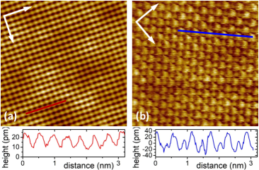
searching. A typical cleaved surface of SmB6 is presented in Figure 4a, obtained with bias voltage 0.2 V and setpoint current 0.5 nA. The height scan shown in Figure 4b, taken along the red line in (a), indicates a roughness of at least a unit cell height and hence, both B and Sm are exposed at the surface. From the involved height changes it appears that the crystal structure may be disturbed within some areas. This raises the question whether such disturbed surface areas can still be considered as weakly disordered and hence, whether the proposed non-trivial surface states remain topologically protected [125]. Nonetheless, there are also some small, flat areas which exhibit corrugations of distance , see orange circle in Figure 4b, which raise hopes for atomic resolution.
Polar surfaces are prone to surface reconstructions. Indeed, upon searching, such reconstructions can often be found [126, 127, 128, 129]. Low-energy electron diffraction (LEED) reported reconstructions [130], mostly of type [131, 132, 133]. The latter can be visualized by a Sm-terminated surface with each other line of Sm atoms missing. Conversely, a B-terminated surface with each second line of B-octahedra missing can be imagined, see Figure 2 in [122]. The topography presented in Figure 4c is consistent with a reconstruction, as is obvious from the distances of in the height scan Figure 4d. The height changes seem more consistent with the former notation of Sm atomic lines missing. In case of such a reconstruction, also domains should be expected and indeed, an example of such a domain is marked by a green arrow in Figure 4c. As expected, we also observed an offset of on a reconstruction (red arrow), further supporting its assignment as a reconstruction. Energetically, however, there is no need for these Sm- (or B-) lines to run straight over extended distances as long as approximately similar amounts of Sm or B-octahedra are exposed at the surface. In result, we also observed bent lines of Sm atoms, Figure 4e. Again, the height change is consistent with Sm on top of a B surface, Figure 4d. The observed step heights render an assignment of the reconstructed surfaces (be it ordered or disordered as in Figure 4e) as a pure, and hence atomically flat, Sm-terminated surface unlikely [129] as it would require a remarkable modulation of the local density of states (DOS). However, the assignment in [129] is merely based on the observation of Sm-based features in tunneling spectroscopy, and our suggestion of Sm on top of B would indeed expose a considerable amount of Sm at the surface. Local differences in tunneling spectroscopy depending on the exposed surface atom have been reported [127, 122] and will be

discussed below, section 5.1. We note that the finding of bent lines of Sm atoms may complicate the interpretation of results which depend on long-range order [134]. Additional complications stem from the reported time dependencies [80, 132, 135]. In particular, patches of reconstructed areas observed a few days after in situ cleave could no longer be resolved after 30 days albeit the sample was kept in UHV and below 20 K [132]. We also wish to point out that two other reconstructions have been reported: i) a surface with only each third line of top Sm atoms missing was presented [124]; ii) on a Sm-deficient sample, a new type of reconstruction, tentatively assigned ()R45∘, was observed [108].
Surface reconstructions could pose a challenge for the study of a conducting surface layer in SmB6. As an example, the Si(111)77 surface is metallic, in contrast to bulk Si [136]. We therefore concentrate on unreconstructed surfaces in the following.
The cubic structure of the hexaborides does not allow for a straightforward distinction of the different surface terminations, especially for atomically flat surfaces [108]. This becomes obvious from Figure 5a where a nice example of a topography with corrugations spaced by is presented, cf. Figure 5b. Yet, it is important to note that these height scan lines were recorded parallel to the main crystallographic direction 100 of the surface shown in Figure 5a. In contrast, the main crystallographic directions 100 and 010, as indicated by black arrows, do not follow the lines of corrugations in Figure 5c. This is better seen in Figure 5d, which is a zoom into c), and hence, the crystallographic alignment of the sample is identical. The height scan in d) is parallel to 110 and indeed, the larger protrusions are spaced by 5.8 nm, as expected. Importantly, in between smaller protrusions can be recognized. A comparison to the crystal structure Figure 3 suggests that the smaller protrusions stem from the apex B(1)-atom on a Sm-terminated surface, cf. the unit cell indicated in Figure 5d by colors corresponding to Figure 3. It should be noted that B-terminated surfaces as in Figure 5a have been reported from time to time [126, 122, 129, 137] but Sm-terminated surfaces analogous to Figure 5c only once [123], cf. Figure 12a. This is consistent with our observation that the latter can be found only extremely rarely while the former is encountered every now and then, and conforms to findings of a x-ray absorption study [135]. An annealed Sm surface did not reveal the intermittent protrusions due to remaining disorder [133]. Compared to the B- and Sm-terminated surfaces, the reconstruction is found somewhat more frequently which is energetically favorable [122, 137].
To scrutinize our assignment of surface terminations, we searched for a step on an otherwise flat surface which exhibits both, a B- and a Sm-termination, as presented in Figure 6. We note that in our study of SmB6, which runs for almost a decade by now, we only encountered two suitable steps emphasizing the importance of acquiring sufficient statistics. The different terminations are immediately apparent when keeping the crystallographic orientation of the sample in mind, which is indicated by the white arrows. Within the higher-up (bright) areas, e.g. below the cyan line, the corrugations run along 110, while some lower (darker) areas exhibit atomic arrangements parallel to the main axes, e.g. near the blue line. The height scans along all lines reveal corrugations with periodicity . In accordance with the assignment above, the bright areas may then correspond to Sm-terminations and the darker ones to B apex atoms. This is nicely confirmed by the height change along the red arrow: along the arrow (note the direction) the height increases by 100 pm, in good agreement with the crystal structure Figure 3. The corrugations within the B-terminated areas are even more pronounced compared to those on Sm-terminations, cf. blue and cyan height scans in Figure 6, as one might expect.
It is important to note that our assignment of surface termination does not directly rely on spectroscopy (of course, the density of states also enters

into height measurements). Our assignment of the B-terminated surface agrees with other reports [123, 122, 129]. Yet, the 2 1 reconstruction is attributed to the Sm-termination [129] primarily based on comparison to photoemission experiments. However, in contrast to Ref. 129 unreconstructed areas were found as patches of some 10 nm in extent at most, 2 1 reconstructed areas up to some 100 nm. Note that large-scale (several m and beyond) STM of atomically flat areas have not been reported so far, including [129], in line with predictions [138]. It is therefore highly unlikely that identical areas can be investigated by STM and photoemission, rather the latter most likely integrates over differently terminated areas [137], possibly including rough ones. In addition, no notion is provided [129] as to why a Sm-terminated surface should form a superstructure. We will discuss differences in the STS spectra on and off the Sm on 2 1 reconstructed surfaces below; such a comparison is missing in Ref. 129. We note that the 2 1 reconstruction should be considered a half-Sm termination [128] which emphasizes the presence of Sm at the surface.
The assignment of Sm- and B-terminated, unreconstructed surfaces here differs from those in Refs. 128, 137. The latter are primarily based on band bending effects. It is argued that Sm atoms in the topmost layer accumulate excess electrons due to the missing B layer on top [137]. This argument has been discussed in detail in Ref. 139 along with the counteracting effect of reduced hybridization at the surface (also caused by the reduced number of neighbouring atoms). This reduced hybridization decreases the Kondo temperature at the surface, , relative to the bulk and implies a shift of the Sm valence at the surface toward Sm3+. Such a shift has been observed in x-ray absorption spectroscopy (XAS) [112, 113, 135] and the reduced [140] conforms to the Kondo breakdown scenario [141, 142]. In consequence, an assignment of the surface termination without relying on band-bending effects appears preferable.
Further support for our assignment of terminations stems from comparison to other hexaborides, section 4.3. It is also important to note that, for a comprehensive assignment of surface terminations, all different terminations should be observed and compared. Differences in STM between flux-grown and floating-zone grown samples have not been detailed. There are several reports of surface relaxation [30, 138]. The corresponding atomic displacements in the direction of the bulk are difficult to observe by STM.
4.2 RE substitutions and defects on SmB6
The hexaborides can not only be synthesized with a variety of elements on the RE site, also numerous substitutions on this site have been reported [144]. Such an additional degree of freedom can give rise to new and intriguing phases and phenomena as, e.g., in the case of Ce1-xRExB6 [145]. It also allows for detailed substitution studies, including a change of the electron count by playing with the ratio of divalent vs. trivalent elements, and enabling element-specific measurements like electron-spin resonance (ESR).
In case of SmB6, the fate of the topological surface states upon Sm substitution is of specific interest. In particular, the breaking of time-reversal symmetry due to magnetic substitution can be considered a valid route towards establishing a non-trivial topology in SmB6. With the proposal of non-trivial topology in EuB6 [146], the series Sm1-xEuxB6 is certainly of topical interest [147, 148, 149]. Other magnetic substitutions include Gd [147, 150, 102, 72, 128], Ce [151] and Fe [152, 153, 128].
Introducing substituents into SmB6 changes the cleavage properties. For our cases of 0.5% and 3% Gd as well as 3% Y substituted samples, less force was required for cleaving and atomically flat areas were found more easily, with the vast majority of the investigated surface areas being reconstructed [72]. As for pure SmB6, unreconstructed surface areas were encountered only rarely. One such area on Sm0.995Gd0.005B6 is shown in Figure 7a. The number of defects counted on all our surfaces of substituted samples was typically slightly less than expected if all defects are caused by substituents. Nonetheless, the comparison to

topographies on pure SmB6 and the spectroscopic results on substituted materials presented in section 5.2, in particular the changing tip properties on Gd-substituted SmB6, suggest these defects to be caused by substituents [72]. For comparison, Figure 7c

reproduces a reconstructed surface area of a Fe-substituted sample as observed in Ref. 137.
Investigation of defects can be helpful in addressing the surface termination. Therefore, we consider Sm-deficient samples [108]. However, the defects can be quite different depending on the SmB6 sample growth method [103, 154, 155]: Compared to the floating-zone grown samples, those grown in Al flux tend to show small crystalline Al inclusions [106], but show a remarkable robustness against Sm deficiency [86, 156, 108]. As an example, a sample with 10% Sm deficiency in the flux turned out with nominal composition Sm0.983B6 [108]. On this sample, a characteristic type of cross-like defects was found, which was extremely rare on surfaces of pure SmB6, see Figures 8a and b, and hence, was attributed to a missing Sm atom below a B-terminated surface. The four B octahedra in the surface adjacent to the empty Sm site can then slightly move into the bulk, which explains their slightly lesser height (10 pm) seen in the height profiles Figure 8c. This result supports our interpretation of the involved surfaces as B-terminated.
4.3 Comparison to other hexaborides
Hexaborides have been investigated by STM very early on. In Figure 9 a La-terminated surface of LaB6 is reproduced from Ref. 157. There are approximately 10% La atoms missing. The defects

consist either of single atom sites or of clusters of more than 15 missing atoms [157]. The overall appearance of this surface is remarkably similar to the Sm-terminated surface of Figure 5c reinforcing our claim of a Sm termination for this surface. The atomic corrugation in Figure 9 was specified to approximately 0.2 Å and atomic esolution was reported to be a rare event, both in line with a more recent report on LaB6 [158] and our observations on SmB6. In addition, reconstructions on LaB6 were shown [158] to closely resemble those on SmB6, Figures 4c and e.
The afore-mentioned terminations, namely the reconstruction, the RE- and B-terminated surface, have also been observed on in situ cleaved PrB6 [159], cf. Figure 10. Again, atomically flat areas extend only over a few (nm)2. As in the case of SmB6, the reconstructed surface is ascribed to parallel rows of Pr ions on top of a B6 lattice (Figures 10a and b), which avoids the buildup of an electrical potential on otherwise polar surfaces [159]. On some of the surfaces, a peak is observed at around V in tunneling spectroscopy. Comparison to PES and DFT results suggests that this feature is related to 4 states and hence, the corresponding surfaces are assigned as Pr terminated [159], Figures 10c and d. Unfortunately, the intermittent B-apex atoms cannot be resolved in the topography, Figure 10d. Surfaces, which do not feature such a peak in spectroscopy, are

considered B-terminated, Figures 10e and f.
A small patch of an atomically flat surface of CeB6 (100) was reported in Ref. 160 without further assignment of its termination; yet, a reconstruction on this particular area appears unlikely.
Similarly, for EuB6 a surface reconstruction has not been reported so far. However, both Eu- and B-terminated surfaces of up to some ten nm in extent were observed [161, 124, 162], again after extensive search. Note the striking similarity between EuB6, Figure 11, and SmB6, Figure 5, backing our findings. B-terminated areas exhibit clear corrugations of distance along the main crystallographic directions, Figure 11a. Some of such areas were found to be free of any visible defect on a ten nm scale allowing for further detailed investigation [161, 162]. On the surface of Figure 11b, the bright spots of distance form a square arrangement along the main crystallographic directions, with smaller protrusions at the square centers. This is seen in the height profile along , which closely resembles Figure 5e. Therefore, these smaller protrusions are likely caused by the apex atom of the B-octahedra between Eu atoms. It should be noted that, again, an atomically flat surface exposing the B(2)-B(5) atoms, i.e. intra-octahedral bond breaking, would result in a regular doughnut pattern as discussed for SmB6.
Impurities at the surface of EuB6 can give rise to circular, large-amplitude oscillations of the local DOS around the impurity [162]. The
hybridization of a spin-split surface state with bulk electronic states leads to a resonance which explains the remarkable response even in real-space topography.
For PrB6, stripe-like, or even more complex, corrugations were observed for small bias voltages 0.4 V [159]. While on very rare occasions similar complex corrugations were found on EuB6, a relation to small bias voltages (or close tip-sample distances) could not be established. In this respect, the very close tip-sample distance used in Figure 11 ( V, 0.5 nA) should be noted.
5 Tunneling Spectroscopy on hexaborides
5.1 Pristine SmB6
The interest in STS stems from the fact that the tunneling conductance d is, within simplifying approximations, proportional to the local DOS and can, in principle, provide insight into aspects of the electronic Green’s function [15]. Early reports of tunneling spectroscopy on hexaborides focused on the formation of the zero-bias gap upon decreasing temperature [163, 164, 165]. Point contact spectroscopy in the tunneling regime of SmB6 indicated a substantial zero-bias DOS even at 0.1 K [166]. The concept of topologically protected surface states, however, was applied to SmB6 only about a decade later [10, 24] fueling a renewed interest in spectroscopy on this material, in particular STS and ARPES.
For an evaluation of Kondo insulators and their suitability as strong three-dimensional topological insulators, the bulk band structure has to be known. In particular, the Kondo hybridization evolving at low temperature was studied revealing a direct hybridization gap of order 20 meV [51, 167, 16, 134, 18, 81, 123, 127], see Figure 12. The gap was shown [127] to close up with a logarithmic -dependence, which is a hallmark of Kondo physics [12, 168, 169]. The Kondo hybridization, however, complicates an interpretation of the STS spectra in terms of a local DOS: In addition to tunneling into the conduction band there is also the possibility to tunnel into 4 quasiparticle states giving rise to a co-tunneling phenomenon [170, 171, 172, 173]. In a simple picture, the tunneling conductance can be described as [174]
| (1) |
where and denote the resonance width and its position in energy, respectively. The asymmetry parameter is related to the probability of tunneling into the 4 quasiparticle states relative to the conduction band, as well as the particle-hole asymmetry of the conduction band [172]. Equation 1 could very nicely describe -data obtained on

clean B-terminated surfaces [127, 140]; somewhat more detailed models [171, 172] were also successfully applied [167, 126, 123, 140], but require more open parameters to be adjusted. This is shown in Figure 12c where the spectra above 40 K were fit by the mere co-tunneling model, while at lower an additional Gaussian was introduced [123], as demonstrated for other 4 Kondo systems [175, 176]. An additional contribution can also be seen, e.g., in Figure S13C of Ref. 128. The hybridization gap obtained ranged between 14–20 meV [165, 167, 127, 140, 128], in line with results of other measurements [166, 17, 20, 16, 134, 18, 21, 155, 177, 178, 179], albeit smaller gaps were also reported [123, 23, 122]. The observation of co-tunneling phenomena also on reconstructed [126] or less well-defined surfaces is consistent with the bulk nature of the underlying Kondo effect.
Before discussing the dd-spectra measured to lowest temperatures we compare spectra obtained at 4.6 K on differently terminated surfaces. Figure 13a compares the STS data for the marked areas in Figure 6, which are up to 1 nm in extent. The only significant difference is a small hump at mV in case of the Sm-terminated surface

patch. Spectra obtained on much larger, atomically flat and clean areas (as those shown in Figures 5) are presented in Figure 13b. Both curves can be fit by Equation 1 yielding 16.5 mV, in line with the hybridization gap width. The -values 0.77/1.16 are smaller/larger than unity for B-/Sm-terminated areas consistent with predominant tunneling into the conduction/4 band. Again, there is a peak at mV on the Sm surface on top of the fit suggesting an origin beyond the co-tunneling phenomenon. This peak, also adumbrated in Figure 12b and Ref. 166, may be related to an excitation resulting from the hybridization of the 4-electron wave function [180, 54] as seen in inelastic neutron scattering, consistent with an assignment to Sm-terminated surfaces.
There is a clear temperature progression of the additional peak evolving upon lowering below 40 K, Figure 12c, see also [167, 126]. Indeed, as summarized in Refs. 81, 156, for most samples temperatures below about 3 K suffice to access their compelling low-temperature properties, but in some cases 1 K is required [81, 181]. Apparently, there are also differences between flux-grown and floating-zone grown samples in the very low- regime, as seen in specific heat and quantum oscillation measurements [109, 106]. In consequence, STS was also conducted down to such low [140, 122, 128].
Figure 14a reproduces -data down to 0.35 K [140] taken on a B-terminated surface and far away from any defect, cf. Figure 5a. The behavior is reminiscent of the one in Figure 12c: The data can nicely be fit by Equation 1 at 20 K, while at lower temperature additional contributions have to be

considered. This is best seen for -data at 0.35 K where at least four Gaussian peaks (gray lines and right scale in Figure 14a) can be fitted in addition to a Fano-type background (blue dashed line) [140]. Note that Gaussians were used here for simplicity as the experimental data do not allow to distinguish between different peak shapes (Gaussian lineshapes are usually associated with randomness, while a Lorentzian lineshape with a relaxation phenomenon). The peak energies are approximately , , and meV. These energies do not change up to 4 K, above which temperature specifically the latter two peaks around zero bias cannot be resolved anymore. Along with the fact that these peaks do not change their positions in energy even close to defects, this suggests that they contain bulk contributions. In this respect it is reassuring that very similar energy positions of these peaks have been observed on less clean surfaces of floating-zone grown samples at 0.1 K [122]. Again, this is in line with these energy positions being determined by the bulk properties of SmB6, which apparently are very similar for differently (flux vs. floating-zone) grown samples. Bulk contributions would also explain why the main peak at meV can even be observed on reconstructed surfaces [126, 123, 127].
Having established a relation of the energies of the main peaks with the SmB6 bulk properties, one may attempt to compare the spectra at lowest to the band structure, Figure 2. The clear loss of spectral weight at energies 20 meV marks the hybridization gap, as seen by a number of spectroscopic tools and is discussed above. The most pronounced peak at meV (also observed in Ref. 126) is very likely related to the weakly dispersive band, which is strongly renormalized. Its position in energy indicates that this peak resides inside the (indirect) Kondo hybridization gap and therefore, it is often referred to as in-gap state [52, 182, 183, 184, 17, 185, 133, 122]. As will be argued below, its weight likely contains contributions beyond a simple co-tunneling model. This peak certainly manifests the properties of the smaller gap of a few meV observed in studies of thermal activation energies [37, 186, 49, 86, 166, 72, 111], which is understood in terms of an indirect bulk gap [45, 64, 187], cf. section 2.2. Such an interpretation is in line with Ref. 171 and supported by the peak’s temperature dependence.
The peak located at around meV may then be related to the second band [25, 30, 31, 122], which is brought about by the crystal field splitting the quartet into two doublets away from the point. These states hybridize only lightly. In comparison to the more strongly hybridized states discussed above, these localized -states may give rise to only small features in the tunneling spectra [132]. Such an interpretation is consistent with the insensitivity of this peak to impurities at the surface or applied magnetic fields up to 12 T [140] and with a small -band width of about 20 meV [188]. Alternatively, this peak may also be caused by flat regions in the band structure. In this case, the small peak intensity might be related to the respective orientation in space with respect to the surface normal. Also, the absorption of a magnetic exciton was proposed, based on peaks observed by inelastic neutron scattering (INS) [54] and Raman [52] experiments at 14 and 16 meV, respectively. Since the surface is metallic, the exciton at the surface has a considerable linewidth and a reduced energy [189]. We note that other types of measurements found features at similar energies but provided different explanations for their origin [16, 20, 190]. The peaks at and meV appear only at temperatures below 7 K and are likely of different origin, as discussed below.
As outlined above, the dominating peak at meV certainly contains some bulk contribution. It is, therefore, not surprising that its -dependence can be compared across different samples and differently terminated surfaces, see Figure 14b including data from Ref. 126, 128, 123. It starts to become observable below about 50 K indicating its relation to the evolving Kondo hybridization upon lowering [167, 127]. A similar -scale was found in transport [14, 83, 86] and other spectroscopic measurements [191, 17, 19, 192, 193].
At 5 K, the peak gains in weight more rapidly compared to 5 K; a similar change of slope is observed in [128], yet not quite as pronounced. At these low temperatures, the existence of metallic surface states has been established [83, 84, 167, 117, 86], suggesting a relation between the increased peak height and the surface states. As outlined in section 2, the Kondo hybridization between Sm localized 4 and itinerant 5 states is a prerequisite for the existence of topologically nontrivial surface states. However, at the surface the Kondo hybridization is reduced due to the reduced screening of the Sm ions [139] resulting in a suppressed Kondo temperature at the surface, a phenomenon usually referred to as surface Kondo breakdown [194, 142]. According to Ref. 142, narrow peaks with strongly -dependent STS spectra near can be regarded as smoking gun evidence for surface Kondo breakdown scenario, cf. Figure 14a. Below , the surface Kondo effect results from gradually increasing hybridization between surface conduction electrons and one of the 4-states giving rise to a weakly dispersive band near [141]. In consequence, we can likely associate the build-up of the Kondo effect at the sample surface with the strong increase of the main peak height at 5–7 K in Figure 14b. The development of a heavy fermion surface state below this temperature is in line with results from magnetothermoelectric measurements [195]. Taken together, the main peak at mV not only contains a bulk contribution, but, at , there is also a surface contribution [140, 128, 27]. This will be further elaborated on in section 5.2 for tunneling spectra obtained with magnetic tips.
This interpretation naturally links the STS results with the finding of metallic surface states below in numerous measurements. In addition, it provides an explanation for the emergence of the two peaks at 2 – 3 meV at , see Figure 14a. With about an order of magnitude smaller than in the bulk, one may expect the Kondo hybridization gap at the surface to be about an order of magnitude smaller than the bulk gap. With the latter (as discussed above) found at meV, the former should be seen at 2 meV, in good agreement with experiment. The association of these two peaks with the surface state, along with a surface contribution to the main peak, is supported by the sensitivity of the peak heights close to impurities, while the peak at mV remains largely unaffected [140].
A powerful way to study the electronic structure of a given material by tunneling spectroscopy is through quasiparticle interference (QPI) [196, 197]. In case of SmB6, QPI was applied to reveal the dispersion of the expected Dirac cones. However, on non-reconstructed surfaces no clear evolution of any QPI pattern was observed [123, 140]. A negligible magnetic field response in Ref. 140 pointed to nonmagnetic impurities and hence, spin-dependent or spin-conserving scattering is expected to dominate [198]. In consequence, backscattering is

suppressed for topologically protected surface states with opposite, in-plane spin directions for and on the Dirac cone. The absence of clear QPI signatures is then consistent with topologically protected surface states [199, 200, 27] and renders a scenario based on mere Rashba splitting less likely [198].
This picture changes on a reconstructed surface, likely

because the defects then are mostly Sm vacancies (cf. Figure 7c) which can locally induce a magnetic moment via the Kondo-hole effect [61, 201, 202, 102]. Along with a small spin polarization out of the surface plane [203] or a weak ferromagnetic out-of-plane component at the surface [204], backscattering is then possible again [205]. Indeed, well-resolved QPI pattern along the Sm chains of a reconstructed surface were reported in Ref. 128, see Figure 15. A scattering vector can clearly be resolved at mV and is distinguished from the Bragg peak at (0,). It exhibits a roughly linear dispersion, as expected for a Dirac cone located at around meV, with an effective Dirac mass of of the bare electron mass [128]. A second cone of less heavy Dirac states, also located at the same energy, is resolved at somewhat larger bias voltages. These findings are strongly in favor of topologically non-trivial surface states.
5.2 Substituted SmB6
Magnetic impurities in topological insulators break time reversal symmetry (TRS) and open a surface band gap near the Dirac point, while TRS protects the surface states against non-magnetic ones, see reviews [11] and [206]. In consequence, several studies have been conducted to compare the impact of non-magnetic and magnetic impurities on the surface states [150, 207, 208, 102, 149] for insight into the surface states. It should also be noted that SmB6 doped with Gd or Eu was also used for electron spin resonance (ESR) investigations [209, 210]. Moreover, Gd- and Fe-substituted samples were investigated in Ref. 128 to identify the reconstructed surface.
In Figure 16, topographies obtained on pristine SmB6, 3% Y substituted SmB6 (denoted SmB6:3%Y) and 0.5% Gd substituted SmB6 are presented [72]. Here, surfaces areas of (8 nm)2 with only few defects and likely of B-termination are studied. Assuming a statistical distribution of the substituents, the defects in (b)/(c) are likely caused by Y/Gd (for Gd, see additional argument below). Tunneling spectra taken along the whole length of the respective blue arrows are reproduced in Figure 16d–f, with spectra labelled #1 collected right on top of the respective defect. The most pronounced change is seen for the main peak at mV: this peak is somewhat reduced at the impurity in pure SmB6, but almost not discernable at a Gd impurity (dashed lines mark and mV). All spectra far away from the impurities nicely match Figure 14a. For quantification, the peak heights at mV and mV are plotted in dependence on distance from the respective impurity in Figures 16g–i. Clearly, the peaks are suppressed at the impurity (by ), but completely recover in similar fashion at distances . Importantly, the suppression of the main peak at mV is significantly more pronounced in both, strength and extent for magnetic Gd.
The recovery of the peak height was described by a theoretical model for surface states around magnetic impurities [211], which assumes Dirac electrons of the supposed topological surface state to be locally coupled to a magnetic impurity through exchange coupling. Intuitively, it describes a local gap opening of the topological surface states due to a magnetic impurity. Within this model, the fit parameters are the strength of the exchange coupling , mostly determined by , its range and the Fermi velocity . Fits to this model, dashed lines in Figures 16g–i, describe the experimentally observed behavior of surface state suppression reasonably well. For the Gd-substituted sample, the fit yields 1.4 meV, 3000 m/s and (Gd) 2.2 nm, while , Y) 1.5 nm on pure (with non-magnetic impurity [140]) and Y-substituted SmB6, respectively. Note that the results above for and are in good agreement with [128], given the main peak energy of mV. This, in concert with the applicability of the exchange coupling model as such, supports an interpretation of the surface states being of topological nature. Note also that within the framework of this model, a peak suppression is not expected for non-magnetic impurities; yet the latter may acquire a (small) magnetic moment through the Kondo hole effect mentioned above.
This model also explains naturally the resistivity behavior of the substituted samples (cf. Figure 1): SmB6:3%Y and SmB6:0.5%Gd show a very similar resistivity plateau below about 4 K, while SmB6:3%Gd does not exhibit any sign of a plateau down to 0.32 K [150, 72]. The resistivity plateau signals a conducting path on the surface due to the metallic surface states. On the former two sample surfaces, the areas with suppressed surface states are small enough in number and size to leave sufficient surface unaffected such that conducting paths can still form and cause the plateau. For SmB6:3%Gd with average distance between Gd substituents of nm, the areas of suppressed surface states coalesce and inhibit a conducting path. The comparison between 3%Gd and 3%Y clearly shows that these areas must be larger (in size and/or number) for magnetic impurities, as confirmed by our STS results.
There is one potential issue with the above approach: The substitution also influences the sample’s Kondo hybridization, which is a prerequisite for

topologically non-trivial surface states. This can, e.g., be seen in the smaller total resistivity change upon cooling for the substituted samples compared to pure SmB6, Figure 1 and [150, 102, 72, 149]. To avoid such an influence on the samples’ bulk, yet keeping the short-range exchange interaction, the surface states should also be suppressed by using a magnetic tip. The result is striking, Figure 17a: The spectrum obtained by a Cr tip does not exhibit any sign of the peak at mV (nor at mV), which is the hallmark of the surface states, while the hybridization still appears (albeit somewhat reduced). This result is in line with the model above, employing an exchange coupling between the magnetic entity (here the Cr tip) and the Dirac electrons. Spin-polarized tunneling alone does not explain this huge reduction in peak height [212, 181, 198]. Note that a magnetic field of 12 T does not notably influence the spectrum, ruling out any possible stray field effect of the magnetic tip. It is also worth mentioning that the spectrum obtained with Cr-tip is rather similar to spectra taken with W-tip at around 20 K [72], i.e. a temperature at which the surface states do not yet manifest themselves in tunneling spectra [123, 140, 128]. This emphasizes that it is indeed the surface state contribution which is mainly suppressed.
Albeit the very same surface was investigated by the two tips used in Figure 17a and great care was taken, it cannot be completely ruled out that different surface areas were investigated causing at least part of the huge changes. In this respect, an observation came to help [72]: Upon scanning a regular W tip over a surface of Gd-substituted SmB6, the tip picked up Gd on occasion, converting it into a magnetic one.

A similar process was observed earlier for STM on Fe1+yTe where excess Fe was picked up [213]. The process of picking up an atom is seen by a corresponding sudden height change in topography. The fact that it was indeed a Gd atom which was picked up is supported by the similarity between spectra obtained with such a modified tip and with Cr-tip (cf. Figures 17a and b) and the observation that these changes were exclusively observed on Gd-substituted sample surfaces, but not on any of the Y-substituted or pure SmB6. What’s more, the tip modification can be reversed. By applying a voltage pulse (typically 10 V) to the tip, the picked-up atom can be removed and the original spectrum is retained, Figure 17b. In this case, the very same surface area (on atomic level) was investigated.
5.3 STS on other hexaborides
EuB6 is a ferromagnetic semimetal [214]. Despite its simple lattice (see Figure 3) and magnetic structure (the state of Eu2+ is isotropic), EuB6 shows two consecutive transitions at about 15.3 K and 12.6 K indicating intriguingly complex magnetic behavior [215]. This behavior was discussed early on within the framework of a so-called magnetic polaron [5], an ordered magnetic cluster resulting from the exchange coupling between the conduction electrons and the local magnetic moments, which gives rise to intrinsically inhomogeneous states (see Ref. 216 for a review). Within a magnetic polaron, the charge carriers are localized while spin-polarizing the local magnetic moments over a finite distance. Once the magnetic polarons overlap, the charge carriers can suddenly delocalize, resulting in a mobility increase and percolation of the charges at . This intriguingly simple model can explain the colossal magnetoresistance (CMR) effect in many materials [217]. In case of EuB6, the magnetic polarons are believed to start forming at around 35–40 K, percolate at and finally merge at [218, 219]. Around , EuB6 exhibits a strong CMR effect [215] because the polarons grow in size and/or number upon applying a magnetic field, in line with the polaronic picture.
STS can be utilized to directly visualize electronic inhomogeneity, i.e. the polaron formation [161]. To this end, Figure 18 (upper row) exhibits STS maps on a B-terminated surface as shown in Figure 11a at 5.6 K, 15 K and 20 K. These temperatures were chosen to cover the whole range, i.e., below, in between, and above and , respectively. As expected for the homogeneous ferromagnetic state below , there is no sign of any electronic inhomogeneity in the spectroscopy map at 5.6 K. Also, the dd-spectra averaged over the different marked areas (including an average over the total area) perfectly overlap, which evidences that homogeneous maps are observed not only at mV as shown, but rather at any bias voltage. The picture is changed dramatically at 20 K where patches of enlarged dd are seen in the spectroscopy map at mV. This voltage was chosen because here, the largest differences in are observed, see dd-spectra averaged over areas marked by rectangles of corresponding color in the map. The enlarged local DOS is attributed to the magnetic polarons. At 20 K, these polarons are well separated and are about 3–-4 nm in extent. Note that polarons of very similar size have been visualized by STM in manganites [220].
At intermediate 15 K, the picture is not as clear-cut, mostly because the local differences in are not as pronounced (see dd-spectra). This is likely related to the system being close to the magnetic transition at which any inhomogeneity is expected to vanish. Nonetheless, there appear to be extended regions of enlarged dd (specifically at mV) which may indicate the expected percolating conducting paths between and . Note that the STS measurements shown here are corroborated by local Hall effect measurements [161].
While in the above investigations it was important to look at clean surfaces, surfaces with impurities showed dd-oscillations of large amplitude due to elastic scattering of electrons [162]. Fourier transform STS and DFT slab calculations point to a band with hole-like dispersion lying approximately 68 meV below and a spin-split surface state band, which stems from the dangling orbitals of the apical boron atom and hybridizes with bulk states near the point.
Similarly, in LaB6 a surface resonance at eV is expected from DFT slab calculations which is composed of B dangling bonds. However, these states turn out difficult to image. At positive bias, the La -orbitals contribute to dd [158]. The B dangling bonds are speculated to also lead to a feature at eV on PrB6 surfaces [159]. In addition, a peak at eV is observed in dd for the Pr-terminated surface of Figure 10d, which is related to the 4 states.
5.4 -spectroscopy
LaB6 is well-known for its very low work function of about 2.7 eV [222] and therefore, is an established cathode material. LaB6 was even suggested as a substrate for STM on weakly conducting thin films [223]. The work function of a clean sample surface can be estimated from the tunneling barrier height involved in STM (note that also the tip work function enters into ). To this end, the dependence of the tunneling current on the tip displacement with respect to the sample has to be measured, which are related by
| (2) |
where is the bare electron mass and . Indeed, a value of 3 eV was obtained on a reconstructed LaB6 surface for a bias voltage set point of 0.2 V [158]; a smaller set point resulted in a smaller [224]. Unfortunately, no data were provided on the studied -range.
On B-terminated surfaces of SmB6, -values between 4.5 eV and 6.7 eV were found [108]. A somewhat larger range of from order of 4 eV up to 7 eV was reported for small (order of 1 nm) patches, with the larger values likely obtained on defects [122]. Based on DFT calculations, the work function of Sm-terminated surfaces should be of order 2 eV, while being at least twice as high on B-terminated surfaces [122], supporting the findings and assignments. These data are confirmed by an early report on SmB6 with very little Sm in the surface layer (4.2 eV, [225]) and more recent ARPES measurements (4.5 eV, [16]). For comparison, the work function of pure Sm is close to 2.7 eV and for pure B about 4.45 eV [226].
For B-terminated EuB6, values of 4.7 eV and 5.6 eV were determined [124], in good agreement with B-terminated SmB6. Unfortunately, there are no values for RE-terminated surfaces given.
6 Modification of the SmB6 surface
For many investigations and applications it is useful to prepare materials in thin film form. Attempts to grow films of hexaborides were made early on, see e.g. Ref. 227, 228, 144. Special efforts have been made for LaB6 because of its low work function, and for SmB6 subsequent to the proposal of non-trivial surface states [229, 230, 231, 232]. One particularly interesting application of a thin film of SmB6 makes use of the proximity effect [233]. Here, superconductivity in SmB6 is

induced by fabricating bilayers of the latter and superconducting Nb thin films. The thickness of the surface state was estimated to be nm.
The surface of SmB6 can be damaged by ion irradiation to different depths [234, 208]. Subsequent resistivity measurements indicated that the surface states form anew in a layer below the damaged material, in line with its non-trivial topology. Using a focused ion beam (FIB), the ion damage can be inflicted in a locally more controlled way [111], see examples in Figure 19. With increasing number of FIB-cut lines, the low- resistivity plateau kicks in at lower temperature and shifts to higher resistivity values likely indicating a confinement of the persisting surface states [133] despite possible disorder effects [235, 236] due to the FIB treatment.
7 Conclusions and Outlook
The exciting variety of physical phenomena observed in hexaborides effectively calls for investigations by such dedicated tools like STM, which provides insight into the density of states, or more generally, into the Green’s function. In particular, requirements like low temperatures, energy resolution on a meV-scale or the possibility of applying magnetic fields can be met by STM. Unfortunately, the cubic crystal structure does not provide a preferred cleaving plane and hence, atomically flat surface areas have to be searched for extensively, and are usually only up a few 100 nm in extent. Both restrictions are even more true if unreconstructed surfaces are strived for. While this behavior is a severe obstacle for STM, it should also be kept in mind in any other surface sensitive technique, e.g. ARPES or point contact spectroscopy.
Nonetheless, atomically flat surface areas can be found, and we here provided an overview of the different surface terminations encountered. Given the common crystal structure, the topographies of the different hexaborides can be nicely compared and, with a sufficiently broad database, the surface terminations can reasonably be assigned. Knowing the surface termination of atomically flat surfaces, i.e. B- vs. RE-terminated or reconstructed, is certainly helpful for any interpretation of STS data.
Tunneling spectroscopy confirmed the Kondo effect in SmB6. At temperatures below a few K, individual peaks beyond a co-tunneling effect can be resolved and a Kondo breakdown at the surface, in line with predictions, is hinted at. Magnetic substituents locally suppress the formation of the surface state, again in line with theory, which is a strong indication for a topologically non-trivial nature of these surface states. Investigating the quasiparticle interference pattern on reconstructed surfaces revealed a linear dispersion as expected for a Dirac cone [128]. On clean EuB6 surfaces, the formation of polarons near the metal-semiconductor transition could directly be visualized.
Finding atomically flat surface areas may fuel renewed interest in STS on other hexaborides. Specifically, CeB6 is certainly worthwhile studying provided sufficiently low temperatures (below about 2 K) are achieved and, preferably, magnetic fields can be applied.
With the availability of hexaboride thin films not only the issues related to the cleavage of hexaborides could be circumvented, but also new phenomena and applications become available for study. An example here is the SmB6/YB6 heterostructure for which Klein tunneling was observed [239]. STM is certainly also helpful if hexaboride nanowires are to be investigated. One may even imagine using sharply pointed SmB6 single crystals as tunneling tips, with the unique spin-momentum locking in the TKI SmB6 likely giving rise to interesting tunneling phenomena.
In addition to materials development, new functionality can also be added to STM. For example, in situ strain devices have been implemented into STM [240]. Such an additional experimental degree of freedom may also provide new insight into hexaborides.
8 Acknowledgements
The authors gratefully acknowledge collaborations and fruitful discussions with Victoria Ale Crivilero, Z. Fisk, Lin Jiao, S. Kirchner, J. Müller, Sahana Rößler, Priscila Rosa, F. Steglich and L. Hao Tjeng. SW acknowledges support by the Deutsche Forschungsgemeinschaft through WI 1324/5-1.
References
- Moissan and Williams [1897] H. Moissan and P. Williams, C. R. Acad. Sci. (Paris) 125, 629 (1897).
- Pauling and Weinbaum [1934] L. Pauling and S. Weinbaum, Z. Kristallogr. 87, 181 (1934).
- Geballe et al. [1968] T. H. Geballe, B. T. Matthias, K. Andres, J. P. Maita, A. S. Cooper, and E. Corenzwit, Science 160, 1443 (1968).
- Nyhus et al. [1997a] P. Nyhus, S. Yoon, M. Kauffman, S. L. Cooper, Z. Fisk, and J. Sarrao, Phys. Rev. B 56, 2717 (1997a).
- Urbano et al. [2004] R. R. Urbano, P. G. Pagliuso, C. Rettori, S. B. Oseroff, J. L. Sarrao, P. Schlottmann, and Z. Fisk, Phys. Rev. B 70, 140401(R) (2004).
- Schell et al. [1982] G. Schell, H. Winter, H. Rietschel, and F. Gompf, Phys. Rev. B 25, 1589 (1982).
- Effantin et al. [1985] J. M. Effantin, J. Rossat-Mignod, P. Burlet, H. Bartholin, S. Kunii, and T. Kasuya, J. Magn. Magn. Mater. 47-48, 145 (1985).
- Zhou et al. [2015] Y. Zhou, D.-J. Kim, P. F. S. Rosa, Q. Wu, J. Guo, S. Zhang, Z. Wang, D. Kang, C. Zhang, W. Yi, et al., Phys. Rev. B 92, 241118(R) (2015).
- Deng et al. [2013] X. Deng, K. Haule, and G. Kotliar, Phys. Rev. Lett. 111, 176404 (2013).
- Dzero et al. [2010] M. Dzero, K. Sun, V. Galitski, and P. Coleman, Phys. Rev. Lett. 104, 106408 (2010).
- Hasan and Kane [2010] M. Z. Hasan and C. L. Kane, Rev. Mod. Phys. 82, 3045 (2010).
- Aeppli and Fisk [1992] G. Aeppli and Z. Fisk, Comments Cond. Mat. Phys. 16, 155 (1992).
- Riseborough [2000a] P. S. Riseborough, Adv. Phys. 49, 257 (2000a).
- Allen et al. [1979] J. W. Allen, B. Batlogg, and P. Wachter, Phys. Rev. B 20, 4807 (1979).
- Kirchner et al. [2020] S. Kirchner, S. Paschen, Q. Chen, S. Wirth, D. Feng, J. D. Thompson, and Q. Si, Rev. Mod. Phys. 92, 011002 (2020).
- Neupane et al. [2013] M. Neupane, N. Alidoust, S.-Y. Xu, T. Kondo, Y. Ishida, D. J. Kim, C. Liu, I. Belopolski, Y. J. Jo, T.-R. Chang, et al., Nat. Commun. 4, 2991 (2013).
- Jiang et al. [2013] J. Jiang, S. Li, T. Zhang, Z. Sun, F. Chen, Z. R. Ye, M. Xu, Q. Q. Ge, S. Y. Tan, X. H. Niu, et al., Nat. Commun. 4, 3010 (2013).
- Xu et al. [2013] N. Xu, X. Shi, P. K. Biswas, C. E. Matt, R. S. Dhaka, Y. Huang, N. C. Plumb, M. Radović, J. H. Dil, E. Pomjakushina, et al., Phys. Rev. B 88, 121102 (2013).
- Xu et al. [2014a] N. Xu, C. E. Matt, E. Pomjakushina, X. Shi, R. S. Dhaka, N. C. Plumb, M. Radović, P. K. Biswas, D. Evtushinsky, V. Zabolotnyy, et al., Phys. Rev. B 90, 085148 (2014a).
- Denlinger et al. [2014] J. D. Denlinger, J. W. Allen, J.-S. Kang, K. Sun, B.-I. Min, D.-J. Kim, and Z. Fisk, JPS Conf. Proc. 3, 017038 (2014).
- Xu et al. [2014b] N. Xu, P. K. Biswas, J. H. Dil, R. S. Dhaka, G. Landolt, S. Muff, C. E. Matt, X. Shi, N. C. Plumb, M. Radović, et al., Nat. Commun. 5, 4566 (2014b).
- Suga et al. [2014] S. Suga, K. Sakamoto, T. Okuda, K. Miyamoto, K. Kuroda, A. Sekiyama, J. Yamaguchi, H. Fujiwara, A. Irizawa, T. Ito, et al., J. Phys. Soc. Jpn. 83, 014705 (2014).
- Hlawenka et al. [2018] P. Hlawenka, K. Siemensmeyer, E. Weschke, A. Varykhalov, J. Sánchez-Barriga, N. Y. Shitsevalova, A. V. Dukhnenko, V. B. Filipov, S. Gabáni, K. Flachbart, et al., Nat. Commun. 9, 517 (2018).
- Takimoto [2011] T. Takimoto, J. Phys. Soc. Jpn. 80, 123710 (2011).
- Lu et al. [2013] F. Lu, J. Zhao, H. Weng, Z. Fang, and X. Dai, Phys. Rev. Lett. 110, 096401 (2013).
- Alexandrov et al. [2013] V. Alexandrov, M. Dzero, and P. Coleman, Phys. Rev. Lett. 111, 226403 (2013).
- Baruselli and Vojta [2014] P. P. Baruselli and M. Vojta, Phys. Rev. B 90, 201106 (2014).
- Baruselli and Vojta [2015] P. P. Baruselli and M. Vojta, Phys. Rev. Lett. 115, 156404 (2015).
- Yu et al. [2015] R. Yu, H. M. Weng, X. Hu, Z. Fang, and X. Dai, New J. Phys. 17, 023012 (2015).
- Kim et al. [2014a] J. Kim, K. Kim, C.-J. Kang, S. Kim, H. C. Choi, J.-S. Kang, J. D. Denlinger, and B. I. Min, Phys. Rev. B 90, 075131 (2014a).
- Kang et al. [2015] C.-J. Kang, J. Kim, K. Kim, J. Kang, J. D. Denlinger, and B. I. Min, J. Phys. Soc. Jpn. 84, 024722 (2015).
- Hundley et al. [1990] M. F. Hundley, P. C. Canfield, J. D. Thompson, Z. Fisk, and J. M. Lawrence, Phys. Rev. B 42, 6842 (1990).
- Meisner et al. [1985] G. P. Meisner, M. S. Torikachvili, K. N. Yang, M. B. Maple, and R. Guertin, J. Appl. Phys. 57, 3073 (1985).
- Paschen et al. [2010] S. Paschen, H. Winkler, T. Nezu, M. Kriegisch, G. Hilschner, J. Custers, A. Prokofiev, and A. Strydom, J. Phys.: Conf. Series 200, 012156 (2010).
- Iga et al. [1988] F. Iga, M. Kasaya, and T. Kasuya, J. Magn. Magn. Mater. 76-77, 156 (1988).
- DiTusa et al. [1997] J. F. DiTusa, K. Friemelt, E. Bucher, G. Aeppli, and A. P. Ramirez, Phys. Rev. Lett. 78, 2831 (1997).
- Menth et al. [1969] A. Menth, E. Buehler, and T. H. Geballe, Phys. Rev. Lett. 22, 295 (1969).
- Maple and Wohlleben [1971] M. B. Maple and D. Wohlleben, Phys. Rev. Lett. 27, 511 (1971).
- Takabatake et al. [1992] T. Takabatake, M. Nagasawa, H. Fujii, G. Hido, M. Nohara, S. Nishigori, T. Suzuki, T. Fujita, R. Helfrich, U. Ahlheim, et al., Phys. Rev. B 45, 5740(R) (1992).
- Izawa et al. [1999] K. Izawa, T. Suzuki, T. Fujita, T. Takabatake, G. Nakamoto, H. Fujii, and K. Maezawa, Phys. Rev. B 59, 2599 (1999).
- Schlesinger et al. [1993] Z. Schlesinger, Z. Fisk, H. T. Zhang, M. B. Maple, J. F. DiTusa, and G. Aeppli, Phys. Rev. Lett. 71, 1748 (1993).
- Cooley et al. [1999] J. C. Cooley, C. H. Mielke, W. L. Hults, J. D. Goettee, M. M. Honold, R. M. Modler, A. Lacerda, D. G. Rickel, and J. L. Smith, J. Supercond. 12, 171 (1999).
- Jaime et al. [2000] M. Jaime, R. Movshovich, G. R. Stewart, W. P. Beyermann, M. Gomez Berisso, M. F. Hundley, P. C. Canfield, and J. L. Sarrao, Nature 405, 160 (2000).
- Sugiyama et al. [1988] K. Sugiyama, F. Iga, M. Kasaya, T. Kasuya, and M. Date, J. Phys. Soc. Jpn. 57, 3946 (1988).
- Cooley et al. [1995a] J. C. Cooley, M. C. Aronson, Z. Fisk, and P. C. Canfield, Phys. Rev. Lett. 74, 1629 (1995a).
- Cooley et al. [1995b] J. C. Cooley, M. C. Aronson, A. Lacerda, Z. Fisk, P. C. Canfield, and R. P. Guertin, Phys. Rev. B 52, 7322 (1995b).
- Barla et al. [2005] A. Barla, J. Derr, J. P. Sanchez, B. Salce, G. Lapertot, B. P. Doyle, R. Rüffer, R. Lengsdorf, M. M. Abd-Elmeguid, and J. Flouquet, Phys. Rev. Lett. 94, 166401 (2005).
- Barla et al. [2004] A. Barla, J. P. Sanchez, Y. Haga, G. Lapertot, B. P. Doyle, O. Leupold, R. Rüffer, M. M. Abd-Elmeguid, R. Lengsdorf, and J. Flouquet, Phys. Rev. Lett. 92, 066401 (2004).
- von Molnár et al. [1982] S. von Molnár, T. Theis, A. Benoit, A. Briggs, J. Flouquet, J. Ravex, and Z. Fisk, in Valence Instabilities, edited by P. Wachter and H. Boppart (North-Holland, Amsterdam, 1982), pp. 389–395.
- Nanba et al. [1993] T. Nanba, H. Ohta, M. Motokawa, S. Kimura, S. Kunii, and T. Kasuya, Physica B 186-8, 440 (1993).
- Gorshunov et al. [1999] B. Gorshunov, N. Sluchanko, A. Volkov, M. Dressel, G. Knebel, A. Loidl, and S. Kunii, Phys. Rev. B 59, 1808 (1999).
- Nyhus et al. [1997b] P. Nyhus, S. L. Cooper, Z. Fisk, and J. Sarrao, Phys. Rev. B 55, 12488 (1997b).
- Alekseev et al. [1993a] P. A. Alekseev, J. M. Mignot, J. Rossat-Mignod, V. N. Lazukov, and I. P. Sadikov, Physica B 186-8, 384 (1993a).
- Alekseev et al. [1995] P. A. Alekseev, J. M. Mignot, J. Rossat-Mignod, V. N. Lazukov, I. P. Sadikov, E. S. Konovalova, and Y. B. Paderno, J. Phys. Condens. Matter 7, 289 (1995).
- Yeo et al. [2003] S. Yeo, S. Nakatsuji, A. D. Bianchi, P. Schlottmann, Z. Fisk, L. Balicas, P. A. Stampe, and R. J. Kennedy, Phys. Rev. Lett. 91, 046401 (2003).
- Sluchanko et al. [2002] N. E. Sluchanko, V. V. Glushkov, S. V. Demishev, A. A. Menovsky, L. Weckhuysen, and V. V. Moshchalkov, Phys. Rev. B 65, 064404 (2002).
- Bouvet et al. [1998] A. Bouvet, T. Kasuya, M. Bonnet, L. P. Regnault, J. Rossat-Mignod, F. Iga, B. Fåk, and A. Severing, J. Phys.: Condens. Matter. 10, 5667 (1998).
- Nefeodova et al. [1999] E. V. Nefeodova, P. A. Alekseev, J.-M. Mignot, V. N. Lazukov, I. P. Sadikov, Y. B. Paderno, N. Y. Shitsevalova, and R. S. Eccleston, Phys. Rev. B 60, 13507 (1999).
- Riseborough [2001] P. S. Riseborough, Phys. Rev. B 63, 064411 (2001).
- Riseborough [2003] P. S. Riseborough, Phys. Rev. B 69, 235213 (2003).
- Sollie and Schlottmann [1991] R. Sollie and P. Schlottmann, J. Appl. Phys. 69, 5478 (1991).
- Schlottmann [1992] P. Schlottmann, Phys. Rev. B 46, 998 (1992).
- Kasuya [1996] T. Kasuya, J. Phys. Soc. Jpn. 65, 2548 (1996).
- Riseborough [2000b] P. S. Riseborough, Ann. Phys. 9, 813 (2000b).
- Moore and Balents [2007] J. E. Moore and L. Balents, Phys. Rev. B 75, 121306(R) (2007).
- Fu et al. [2007] L. Fu, C. L. Kane, and E. J. Mele, Phys. Rev. Lett. 98, 106803 (2007).
- Hsieh et al. [2008] D. Hsieh, D. Qian, L. Wray, Y. Xia, Y. S. Hor, R. J. Cava, and M. Z. Hasan, Nature 452, 970 (2008).
- Roy [2009] R. Roy, Phys. Rev. B 79, 195321 (2009).
- Dzero et al. [2016] M. Dzero, J. Xia, V. Galitski, and P. Coleman, Annu. Rev. Condens. Matter Phys. 7, 249 (2016).
- Wakeham et al. [2016a] N. Wakeham, P. F. S. Rosa, Y. Q. Wang, M. Kang, Z. Fisk, F. Ronning, and J. D. Thompson, Phys. Rev. B 94, 035127 (2016a).
- Hagiwara et al. [2016] K. Hagiwara, Y. Ohtsubo, M. Matsunami, S.-i. Ideta, K. Tanaka, H. Miyazaki, J. E. Rault, P. Le Fèvre, F. Bertran, A. Taleb-Ibrahimi, et al., Nat. Commun. 7, 12690 (2016).
- Jiao et al. [2018] L. Jiao, S. Rößler, D. Kasinathan, P. F. S. Rosa, C. Guo, H. Yuan, C.-X. Liu, Z. Fisk, F. Steglich, and S. Wirth, Sci. Adv. 4, eaau4886 (2018).
- Vainshtein et al. [1965] E. E. Vainshtein, S. M. Blokhin, and Y. B. Paderno, Sov. Phys.-Solid State 6, 2318 (1965).
- Sluchanko et al. [1999] N. E. Sluchanko, A. A. Volkov, V. V. Glushkov, B. P. Gorshunov, S. V. Demishev, M. V. Kondrin, A. A. Pronin, and N. A. Samarin, J. Exp. Theor. Phys. 88, 533 (1999).
- Cohen et al. [1970] R. L. Cohen, M. Eibschütz, and K. W. West, Phys. Rev. Lett. 24, 383 (1970).
- Takigawa et al. [1981] M. Takigawa, H. Yasuoka, Y. Kitaoka, T. Tanaka, H. Nozaki, and Y. Ishizawa, J. Phys. Soc. Jpn. 50, 2525 (1981).
- Schlottmann [2014] P. Schlottmann, Phys. Rev. B 90, 165127 (2014).
- Glushkov et al. [2006] V. V. Glushkov, A. V. Kuznetsov, O. A. Churkin, S. V. Demishev, Y. B. Paderno, N. Y. Shitsevalova, and N. E. Sluchanko, Physica B 378-380, 614 (2006).
- Thomas et al. [2016] S. Thomas, D. J. Kim, S. B. Chung, T. Grant, Z. Fisk, and J. Xia, Phys. Rev. B 94, 205114 (2016).
- Zhu et al. [2013] Z.-H. Zhu, A. Nicolaou, G. Levy, N. P. Butch, P. Syers, X. F. Wang, J. Paglione, G. A. Sawatzky, I. S. Elfimov, and A. Damascelli, Phys. Rev. Lett. 111, 216402 (2013).
- Denlinger et al. [2013] J. D. Denlinger, J. W. Allen, J.-S. Kang, K. Sun, J.-W. Kim, J. H. Shim, B. I. Min, D.-J. Kim, and Z. Fisk, Temperature dependence of linked gap and surface state evolution in the mixed valent topological insulator SmB6, (Preprint) arXiv:1312.6637 (2013).
- Hsieh et al. [2009] D. Hsieh, Y. Xia, D. Qian, L. Wray, J. H. Dil, F. Meier, J. Osterwalder, L. Patthey, J. G. Checkelsky, N. P. Ong, et al., Nature 460, 1101 (2009).
- Wolgast et al. [2013] S. Wolgast, C. Kurdak, K. Sun, J. W. Allen, D.-J. Kim, and Z. Fisk, Phys. Rev. B 88, 180405(R) (2013).
- Kim et al. [2013] D. J. Kim, S. Thomas, T. Grant, J. Botimer, Z. Fisk, and J. Xia, Sci. Rep. 3, 3150 (2013).
- Eo et al. [2018] Y. S. Eo, K. Sun, C. Kurdak, D.-J. Kim, and Z. Fisk, Phys. Rev. Appl. 9, 044006 (2018).
- Eo et al. [2019] Y. S. Eo, A. Rakoski, J. Lucien, D. Mihaliov, C. Kurdak, P. F. S. Rosa, and Z. Fisk, Proc. Natl. Acad. Sci. USA 116, 12638 (2019).
- Kim et al. [2012] D. J. Kim, T. Grant, and Z. Fisk, Phys. Rev. Lett. 109, 096601 (2012).
- Stern et al. [2016] A. Stern, D. K. Efimkin, V. Galitski, Z. Fisk, and J. Xia, Phys. Rev. Lett. 116, 166603 (2016).
- Casas et al. [2018] B. Casas, A. Stern, D. K. Efimkin, Z. Fisk, and J. Xia, Phys. Rev. B 97, 035121 (2018).
- Stankiewicz et al. [2021] J. Stankiewicz, J. Blasco, P. Schlottmann, M. Ciomaga Hatnean, and G. Balakrishnan, Impedance spectroscopy of SmB6 single crystals, (Preprint) arXiv:2109.05313 (2021).
- Cahill and Graeve [2019] J. T. Cahill and O. A. Graeve, J. Mater. Res. Technol. 8, 6321 (2019).
- Berrada et al. [1978] A. Berrada, J. P. Mercurio, J. Etourneau, P. Hagenmuller, and A. M. Shroff, J. Less-Common Met. 59, 7 (1978).
- Mercurio et al. [1976] J. P. Mercurio, J. Etourneau, R. Naslain, and P. Hagenmuller, J. Less-Common Met. 47, 175 (1976).
- Massidda et al. [1996] S. Massidda, A. Continenza, T. M. de Pascale, and R. Monnier, Z. Phys. B 102, 83 (1996).
- Ahmed and Broers [1972] H. Ahmed and A. N. Broers, J. Appl. Phys. 43, 2185 (1972).
- Canfield and Fisk [1992] P. C. Canfield and Z. Fisk, Philos. Mag. B 65, 1117 (1992).
- Rosa and Fisk [2018] P. F. S. Rosa and Z. Fisk, in Crystal Growth of Intermetallics, edited by P. Gille and Y. Grin (Berlin, Boston: De Gruyter, 2018), pp. 49–60.
- Tanaka et al. [1980] T. Tanaka, R. Nishitani, C. Oshima, E. Bannai, and S. Kawai, J. Appl. Phys. 51, 3877 (1980).
- Paderno et al. [1981] Y. B. Paderno, V. I. Lazorenko, and A. V. Kovalev, Powder Metall. Met. Ceram. 20, 717 (1981).
- Ciomaga Hatnean et al. [2013] M. Ciomaga Hatnean, M. R. Lees, D. M. Paul, and G. Balakrishnan, Sci. Rep. 3, 3071 (2013).
- Prokofiev [2018] A. Prokofiev, in Crystal Growth of Intermetallics, edited by P. Gille and Y. Grin (Berlin, Boston: De Gruyter, 2018), pp. 91–116.
- Fuhrman et al. [2018] W. T. Fuhrman, J. R. Chamorro, P. Alekseev, J.-M. Mignot, T. Keller, J. A. Rodriguez-Rivera, Y. Qiu, P. Nikolić, T. M. McQueen, and C. L. Broholm, Nat. Commun. 9, 1539 (2018).
- Phelan et al. [2016] W. A. Phelan, S. M. Koohpayeh, P. Cottingham, J. A. Tutmaher, J. C. Leiner, M. D. Lumsden, C. M. Lavelle, X. P. Wang, C. Hoffmann, M. A. Siegler, et al., Sci. Rep. 6, 20860 (2016).
- Orendáč et al. [2017] M. Orendáč, S. Gabáni, G. Pristáš, E. Gažo, P. Diko, P. Farkašovský, A. Levchenko, N. Shitsevalova, and K. Flachbart, Phys. Rev. B 96, 115101 (2017).
- Eo et al. [2021] Y. S. Eo, A. Rakoski, S. Sinha, D. Mihaliov, W. T. Fuhrman, S. R. Saha, P. F. S. Rosa, Z. Fisk, M. Ciomaga Hatnean, G. Balakrishnan, et al., Phys. Rev. Materials 5, 055001 (2021).
- Thomas et al. [2019] S. Thomas, X. Ding, F. Ronning, V. Zapf, J. Thompson, Z. Fisk, J. Xia, and P. Rosa, Phys. Rev. Lett. 122, 166401 (2019).
- Grushko et al. [1985] Y. S. Grushko, Y. B. Paderno, K. Y. Mishin, L. I. Molkanov, G. A. Shadrina, E. S. Konovalova, and E. M. Dudnik, Phys. Stat. Sol. B 128, 591 (1985).
- Ale Crivillero et al. [2021a] M. V. Ale Crivillero, S. Rößler, H. Borrmann, H. Dawczak-Dȩbicki, P. F. S. Rosa, Z. Fisk, and S. Wirth, Phys. Rev. Materials 5, 044204 (2021a).
- Hartstein et al. [2018] M. Hartstein, H. W. Toews, Y.-T. Hsu, B. Zeng, X. Chen, M. Ciomaga Hatnean, Q. R. Zhang, S. Nakamura, A. S. Padgett, G. Rodway-Gant, et al., Nat. Phys. 14, 166 (2018).
- Eo et al. [2020] Y. S. Eo, S. Wolgast, A. Rakoski, D. Mihaliov, B. Y. Kang, M. S. Song, B. K. Cho, M. Ciomaga Hatnean, G. Balakrishnan, Z. Fisk, et al., Phys. Rev. B 101, 155109 (2020).
- Ale Crivillero et al. [2021b] M. V. Ale Crivillero, M. König, J. C. Souza, P. G. Pagliuso, J. Sichelschmidt, P. F. S. Rosa, Z. Fisk, and S. Wirth, Phys. Rev. Research 3, 023162 (2021b).
- Lutz et al. [2016] P. Lutz, M. Thees, T. R. F. Peixoto, B. Y. Kang, B. K. Cho, C.-H. Min, and F. Reinert, Philos. Mag. 96, 3307 (2016).
- Utsumi et al. [2017] Y. Utsumi, D. Kasinathan, K.-T. Ko, S. Agrestini, M. W. Haverkort, S. Wirth, Y.-H. Wu, K.-D. Tsuei, D.-J. Kim, Z. Fisk, et al., Phys. Rev. B 96, 155130 (2017).
- Trenary [2012] M. Trenary, Sci. Technol. Adv. Mater. 13, 023002 (2012).
- Bellucci et al. [2019] A. Bellucci, M. Mastellone, S. Orlando, M. Girolami, A. Generosi, B. Paci, P. Soltani, A. Mezzi, S. Kaciulis, R. Polini, et al., Appl. Surf. Sci. 479, 296 (2019).
- Wolgast et al. [2015] S. Wolgast, Y. S. Eo, T. Öztürk, G. Li, Z. Xiang, C. Tinsman, T. Asaba, B. Lawson, F. Yu, J. W. Allen, et al., Phys. Rev. B 92, 115110 (2015).
- Syers et al. [2015] P. Syers, D. Kim, M. Fuhrer, and J. Paglione, Phys. Rev. Lett. 114, 096601 (2015).
- Biswas et al. [2017] S. Biswas, M. Ciomaga Hatnean, G. Balakrishnan, and A. Bid, Phys. Rev. B 95, 205403 (2017).
- Fuhrman et al. [2019] W. T. Fuhrman, J. C. Leiner, J. W. Freeland, M. van Veenendaal, S. M. Koohpayeh, W. A. Phelan, T. M. McQueen, and C. Broholm, Phys. Rev. B 99, 020401(R) (2019).
- Hess et al. [1989] H. F. Hess, R. B. Robinson, R. C. Dynes, J. M. Valles, Jr., and J. V. Waszczak, Phys. Rev. Lett. 62, 214 (1989).
- Rößler et al. [2016] S. Rößler, L. Jiao, D. J. Kim, S. Seiro, K. Rasim, F. Steglich, L. H. Tjeng, Z. Fisk, and S. Wirth, Philos. Mag. 96, 3262 (2016).
- Sun et al. [2018] Z. Sun, A. Maldonado, W. S. Paz, D. S. Inosov, A. P. Schnyder, J. J. Palacios, N. Y. Shitsevalova, V. B. Filipov, and P. Wahl, Phys. Rev. B 97, 235107 (2018).
- Ruan et al. [2014] W. Ruan, C. Ye, M. Guo, F. Chen, X. Chen, G.-M. Zhang, and Y. Wang, Phys. Rev. Lett. 112, 136401 (2014).
- Wirth et al. [2021] S. Wirth, S. Rößler, L. Jiao, M. V. Ale Crivillero, P. F. S. Rosa, and Z. Fisk, Phys. Status Solidi B 258, 2000022 (2021).
- Schubert et al. [2012] G. Schubert, H. Fehske, L. Fritz, and M. Vojta, Phys. Rev. B 85, 201105(R) (2012).
- Yee et al. [2013] M. M. Yee, Y. He, A. Soumyanarayanan, D.-J. Kim, Z. Fisk, and J. E. Hoffman, Imaging the Kondo insulating gap on SmB6, (Preprint) arXiv:1308.1085 (2013).
- Rößler et al. [2014] S. Rößler, T.-H. Jang, D. J. Kim, L. H. Tjeng, Z. Fisk, F. Steglich, and S. Wirth, Proc. Natl. Acad. Sci. USA 111, 4798 (2014).
- Pirie et al. [2020] H. Pirie, Y. Liu, A. Soumyanarayanan, P. Chen, Y. He, M. M. Yee, P. F. S. Rosa, J. D. Thompson, D.-J. Kim, Z. Fisk, et al., Nat. Phys. 16, 52 (2020).
- Herrmann et al. [2020] H. Herrmann, P. Hlawenka, K. Siemensmeyer, E. Weschke, J. Sánchez-Barriga, A. Varykhalov, N. Y. Shitsevalova, A. V. Dukhnenko, V. B. Filipov, S. Gabáni, et al., Adv. Mater. 32, 1906725 (2020).
- Aono et al. [1978] M. Aono, R. Nishitani, T. Tanaka, E. Bannai, and S. Kawai, Solid State Commun. 28, 409 (1978).
- Miyazaki et al. [2012] H. Miyazaki, T. Hajiri, T. Ito, S. Kunii, and S. I. Kimura, Phys. Rev. B 86, 075105 (2012).
- Ramankutty et al. [2016] S. V. Ramankutty, N. de Jong, Y. K. Huang, B. Zwartsenberg, F. Massee, T. V. Bay, M. S. Golden, and E. Frantzeskakis, J. Electron Spectrosc. Relat. Phenom. 208, 43 (2016).
- Miyamachi et al. [2017] T. Miyamachi, S. Suga, M. Ellguth, C. Tusche, C. M. Schneider, F. Iga, and F. Komori, Sci. Rep. 7, 12837 (2017).
- Frantzeskakis et al. [2013] E. Frantzeskakis, N. de Jong, B. Zwartsenberg, Y. K. Huang, Y. Pan, X. Zhang, J. X. Zhang, F. X. Zhang, L. H. Bao, O. Tegus, et al., Phys. Rev. X 3, 041024 (2013).
- Zabolotnyy et al. [2018] V. B. Zabolotnyy, K. Fürsich, R. J. Green, P. Lutz, K. Treiber, C.-H. Min, A. V. Dukhnenko, N. Y. Shitsevalova, V. B. Filipov, B. Y. Kang, et al., Phys. Rev. B 97, 205416 (2018).
- Yoo and Weitering [2002] K. Yoo and H. H. Weitering, Phys. Rev. B 65, 115424 (2002).
- Matt et al. [2020] C. E. Matt, H. Pirie, A. Soumyanarayanan, Y. He, M. M. Yee, P. Chen, Y. Liu, D. T. Larson, W. S. Paz, J. J. Palacios, et al., Phys. Rev. B 101, 085142 (2020).
- Schmidt et al. [2018] K. M. Schmidt, O. Jaime, J. T. Cahill, D. Edwards, S. T. Misture, O. A. Graeve, and V. R. Vasquez, Acta Mater. 144, 187 (2018).
- Allen [2016] J. W. Allen, Philos. Mag. 96, 3227 (2016).
- Jiao et al. [2016] L. Jiao, S. Rößler, D. J. Kim, L. H. Tjeng, Z. Fisk, F. Steglich, and S. Wirth, Nat. Commun. 7, 13762 (2016).
- Erten et al. [2016] O. Erten, P. Ghaemi, and P. Coleman, Phys. Rev. Lett. 116, 046403 (2016).
- Peters et al. [2016] R. Peters, T. Yoshida, H. Sakakibara, and N. Kawakami, Phys. Rev. B 93, 235159 (2016).
- Denlinger et al. [2016] J. D. Denlinger, S. Jang, G. Li, L. Chen, B. J. Lawson, T. Asaba, C. Tinsman, F. Yu, K. Sun, J. W. Allen, et al., Consistency of photoemission and quantum oscillations for surface states of SmB6, (Preprint) arXiv:1601.07408 (2016).
- Inosov [2021] D. S. Inosov, ed., Rare-earth borides (Jenny Stanford Publishing, Singapore, 2021).
- Nikitin et al. [2018] S. E. Nikitin, P. Y. Portnichenko, A. V. Dukhnenko, N. Y. Shitsevalova, V. B. Filipov, Y. Qiu, J. A. Rodriguez-Rivera, J. Ollivier, and D. S. Inosov, Phys. Rev. B 97, 075116 (2018).
- Nie et al. [2020] S. Nie, Y. Sun, F. B. Prinz, Z. Wang, H. Weng, Z. Fang, and X. Dai, Phys. Rev. Lett. 124, 076403 (2020).
- Geballe [1970] T. H. Geballe, J. Appl. Phys. 41, 904 (1970).
- Yeo et al. [2012] S. Yeo, K. Song, N. Hur, Z. Fisk, and P. Schlottmann, Phys. Rev. B 85, 115125 (2012).
- Miao et al. [2021] L. Miao, C.-H. Min, Y. Xu, Z. Huang, E. C. Kotta, R. Basak, M. Song, B. Kang, B. Cho, K. Kißner, et al., Phys. Rev. Lett. 126, 136401 (2021).
- Kim et al. [2014b] D. J. Kim, J. Xia, and Z. Fisk, Nat. Mater. 13, 466 (2014b).
- Ciomaga Hatnean et al. [2020] M. Ciomaga Hatnean, T. Ahmad, M. Walker, M. R. Lees, and G. Balakrishnan, Crystals 10, 827 (2020).
- Altshuler et al. [2005] T. S. Altshuler, M. S. Bresler, and Y. V. Goryunov, JETP Lett. 81, 475 (2005).
- Akintola et al. [2017] K. Akintola, A. Pal, M. Potma, S. R. Saha, X. F. Wang, J. Paglione, and J. E. Sonier, Phys. Rev. B 95, 245107 (2017).
- Gabáni et al. [2016] S. Gabáni, M. Orendáč, G. Pristáš, E. Gažo, P. Diko, and S. Piovarči, Philos. Mag. 96, 3274 (2016).
- Valentine et al. [2016] M. E. Valentine, S. Koohpayeh, W. A. Phelan, T. M. McQueen, P. F. S. Rosa, Z. Fisk, and N. Drichko, Phys. Rev. B 94, 075102 (2016).
- Li et al. [2020] L. Li, K. Sun, C. Kurdak, and J. W. Allen, Nat. Rev. Phys. 2, 463 (2020).
- Ozcomert and Trenary [1992] J. S. Ozcomert and M. Trenary, Surf. Sci. Lett. 265, L227 (1992).
- Buchsteiner et al. [2019] P. Buchsteiner, F. Sohn, J. G. Horstmann, J. Voigt, M. Ciomaga Hatnean, G. Balakrishnan, C. Ropers, P. E. Blöchl, and M. Wenderoth, Phys. Rev. B 100, 205407 (2019).
- Buchsteiner et al. [2020] P. Buchsteiner, L. Harmsen, M. Ciomaga Hatnean, G. Balakrishnan, and M. Wenderoth, Phys. Rev. B 102, 205403 (2020).
- Enayat [2014] M. Enayat, Ph.D. thesis, École Polytechnique Fédérale de Lausanne, Switzerland (2014).
- Pohlit et al. [2018] M. Pohlit, S. Rößler, Y. Ohno, H. Ohno, S. von Molnár, Z. Fisk, J. Müller, and S. Wirth, Phys. Rev. Lett. 120, 257201 (2018).
- Rößler et al. [2020] S. Rößler, L. Jiao, S. Seiro, P. F. S. Rosa, Z. Fisk, U. K. Rößler, and S. Wirth, Phys. Rev. B 101, 235421 (2020).
- Güntherodt et al. [1982] G. Güntherodt, W. A. Thompson, F. Holtzberg, and Z. Fisk, Phys. Rev. Lett. 49, 1030 (1982).
- Baťková et al. [2008] M. Baťková, I. Baťko, E. S. Konovalova, and N. Shitsevalova, Acta Phys. Pol. A 113, 255 (2008).
- Amsler et al. [1998] B. Amsler, Z. Fisk, J. L. Sarrao, S. von Molnár, M. W. Meisel, and F. Sharifi, Phys. Rev. B 57, 8747 (1998).
- Flachbart et al. [2001] K. Flachbart, K. Gloos, E. Konovalova, Y. Paderno, M. Reiffers, P. Samuely, and P. Švec, Phys. Rev. B 64, 085104 (2001).
- Zhang et al. [2013] X. Zhang, N. P. Butch, P. Syers, S. Ziemak, R. L. Greene, and J. Paglione, Phys. Rev. X 3, 011011 (2013).
- Costi [2000] T. A. Costi, Phys. Rev. Lett. 85, 1504 (2000).
- Wirth and Steglich [2016] S. Wirth and F. Steglich, Nat. Rev. Mat. 1, 16051 (2016).
- Fano [1961] U. Fano, Phys. Rev. 124, 1866 (1961).
- Maltseva et al. [2009] M. Maltseva, M. Dzero, and P. Coleman, Phys. Rev. Lett. 103, 206402 (2009).
- Figgins and Morr [2010] J. Figgins and D. K. Morr, Phys. Rev. Lett. 104, 187202 (2010).
- Wölfle et al. [2010] P. Wölfle, Y. Dubi, and A. V. Balatsky, Phys. Rev. Lett. 105, 246401 (2010).
- Schiller and Hershfield [2000] A. Schiller and S. Hershfield, Phys. Rev. B 61, 9036 (2000).
- Ernst et al. [2011] S. Ernst, S. Kirchner, C. Krellner, C. Geibel, G. Zwicknagl, F. Steglich, and S. Wirth, Nature 474, 362 (2011).
- Aynajian et al. [2012] P. Aynajian, E. H. da Silva Neto, A. Gyenis, R. E. Baumbach, J. D. Thompson, Z. Fisk, E. D. Bauer, and A. Yazdani, Nature 486, 201 (2012).
- Arab et al. [2016] A. Arab, A. X. Gray, S. Nemšák, D. V. Evtushinsky, C. M. Schneider, D.-J. Kim, Z. Fisk, P. F. S. Rosa, T. Durakiewicz, and P. S. Riseborough, Phys. Rev. B 94, 235125 (2016).
- Sun et al. [2017] L. Sun, D.-J. Kim, Z. Fisk, and W. K. Park, Phys. Rev. B 95, 195129 (2017).
- Zhang et al. [2018] J. Zhang, J. Yong, I. Takeuchi, R. L. Greene, and R. D. Averitt, Phys. Rev. B 97, 155119 (2018).
- Alekseev et al. [1993b] P. A. Alekseev, V. N. Lazukov, R. Osborn, B. D. Rainford, I. P. Sadikov, E. S. Konovalova, and Y. B. Paderno, Europhys. Lett. 23, 347 (1993b).
- Kim et al. [2019] J. Kim, C. Jang, X. Wang, J. Paglione, S. Hong, J. Lee, H. Choi, and D. Kim, Phys. Rev. B 99, 245148 (2019).
- Gabáni et al. [1999] S. Gabáni, K. Flachbart, P. Farkašovský, V. Pavlík, I. Bat’ko, T. Herrmannsdörfer, E. Konovalova, and Y. Paderno, Physica B 259, 345 (1999).
- Sluchanko et al. [2000] N. E. Sluchanko, V. V. Glushkov, B. P. Gorshunov, S. V. Demishev, M. V. Kondrin, A. A. Pronin, A. A. Volkov, A. K. Savchenko, G. Grüner, Y. Bruynseraede, et al., Phys. Rev. B 61, 9906 (2000).
- Gabáni et al. [2001] S. Gabáni, K. Flachbart, E. Konovalova, M. Orendáč, Y. Paderno, V. Pavlík, and J. Šebek, Solid State Comm. 117, 641 (2001).
- Xu et al. [2016] N. Xu, H. Ding, and M. Shi, J. Phys.: Condens. Matter 28, 363001 (2016).
- Allen and Martin [1980] J. W. Allen and R. M. Martin, J. Phys. Colloq. C5, 171 (1980).
- Chen et al. [2015] F. Chen, C. Shang, Z. Jin, D. Zhao, Y. P. Wu, Z. J. Xiang, Z. C. Xia, A. F. Wang, X. G. Luo, T. Wu, et al., Phys. Rev. B 91, 205133 (2015).
- Amorese et al. [2019] A. Amorese, O. Stockert, K. Kummer, N. B. Brookes, D.-J. Kim, Z. Fisk, M. W. Haverkort, P. Thalmeier, L. H. Tjeng, and A. Severing, Phys. Rev. B 100, 241107(R) (2019).
- Kapilevich et al. [2015] G. A. Kapilevich, P. S. Riseborough, A. X. Gray, M. Gulacsi, T. Durakiewicz, and J. L. Smith, Phys. Rev. B 92, 085133 (2015).
- Fuhrman et al. [2015] W. T. Fuhrman, J. Leiner, P. Nikolić, G. E. Granroth, M. B. Stone, M. D. Lumsden, L. DeBeer-Schmitt, P. A. Alekseev, J.-M. Mignot, S. M. Koohpayeh, et al., Phys. Rev. Lett. 114, 036401 (2015).
- Caldwell et al. [2007] T. Caldwell, A. P. Reyes, W. G. Moulton, P. L. Kuhns, M. J. R. Hoch, P. Schlottmann, and Z. Fisk, Phys. Rev. B 75, 075106 (2007).
- Park et al. [2016] W. K. Park, L. Sun, A. Noddings, D.-J. Kim, Z. Fisk, and L. H. Greene, Proc. Natl. Acad. Sci. USA 113, 6599 (2016).
- Min et al. [2017] C.-H. Min, F. Goth, P. Lutz, H. Bentmann, B. Y. Kang, B. K. Cho, J. Werner, K.-S. Chen, F. Assaad, and F. Reinert, Sci. Rep. 7, 11980 (2017).
- Alexandrov et al. [2015] V. Alexandrov, P. Coleman, and O. Erten, Phys. Rev. Lett. 114, 177202 (2015).
- Luo et al. [2015] Y. Luo, H. Chen, J. Dai, Z. Xu, and J. D. Thompson, Phys. Rev. B 91, 075130 (2015).
- Petersen et al. [1998] L. Petersen, P. T. Sprunger, P. Hofmann, E. Lægsgaard, B. G. Briner, M. Doering, H.-P. Rust, A. M. Bradshaw, F. Besenbacher, and E. W. Plummer, Phys. Rev. B 57, R6858 (1998).
- Hoffman [2011] J. E. Hoffman, Rep. Prog. Phys. 74, 124513 (2011).
- Oka et al. [2014] H. Oka, O. O. Brovko, M. Corbetta, V. S. Stepanyuk, D. Sander, and J. Kirschner, Rev. Mod. Phys. 86, 1127 (2014).
- Zhang et al. [2009] T. Zhang, P. Cheng, X. Chen, J.-F. Jia, X. Ma, K. He, L. Wang, H. Zhang, X. Dai, Z. Fang, et al., Phys. Rev. Lett. 103, 266803 (2009).
- Guo and Franz [2010] H. M. Guo and M. Franz, Phys. Rev. B 81, 041102 (2010).
- Thompson [2011] J. D. Thompson, Proc. Natl. Acad. Sci. USA 108, 18191 (2011).
- Figgins and Morr [2011] J. Figgins and D. K. Morr, Phys. Rev. Lett. 107, 066401 (2011).
- Baum and Stern [2012] Y. Baum and A. Stern, Phys. Rev. B 85, 121105 (2012).
- Nakajima et al. [2015] Y. Nakajima, P. Syers, X. Wang, R. Wang, and J. Paglione, Nature Phys. 12, 213 (2015).
- Okada et al. [2011] Y. Okada, C. Dhital, W. Zhou, E. D. Huemiller, H. Lin, S. Basak, A. Bansil, Y.-B. Huang, H. Ding, Z. Wang, et al., Phys. Rev. Lett. 106, 206805 (2011).
- Teng et al. [2019] J. Teng, N. Liu, and Y. Li, J. Semicond. 40, 081507 (2019).
- Kang et al. [2016] B. Y. Kang, C.-H. Min, S. S. Lee, M. S. Song, K. K. Cho, and B. K. Cho, Phys. Rev. B 94, 165102 (2016).
- Wakeham et al. [2016b] N. Wakeham, J. Wen, Y. Q. Wang, Z. Fisk, F. Ronning, and J. D. Thompson, J. Magn. Magn. Mater. 400, 62 (2016b).
- Lesseux et al. [2017] G. G. Lesseux, P. F. S. Rosa, Z. Fisk, P. Schlottmann, P. G. Pagliuso, R. R. Urbano, and C. Rettori, AIP Adv. 7, 055709 (2017).
- Demishev et al. [2018] S. V. Demishev, M. I. Gilmanov, A. N. Samarin, A. V. Semeno, N. E. Sluchanko, N. A. Samarin, A. V. Bogach, N. Y. Shitsevalova, V. B. Filipov, M. S. Karasev, et al., Sci. Rep. 8, 7125 (2018).
- Liu et al. [2009] Q. Liu, C.-X. Liu, C. Xu, X.-L. Qi, and S.-C. Zhang, Phys. Rev. Lett. 102, 156603 (2009).
- Baruselli and Vojta [2016] P. P. Baruselli and M. Vojta, Phys. Rev. B 93, 195117 (2016).
- Enayat et al. [2014] M. Enayat, Z. Sun, U. R. Singh, R. Aluru, S. Schmaus, A. Yaresko, Y. Liu, C. Lin, V. Tsurkan, A. Loidl, et al., Science 345, 653 (2014).
- Fisk et al. [1979] Z. Fisk, D. C. Johnston, B. Cornut, S. von Molnár, S. Oseroff, and R. Calvo, J. Appl. Phys. 50, 1911 (1979).
- Süllow et al. [2000] S. Süllow, I. Prasad, M. C. Aronson, S. Bogdanovich, J. L. Sarrao, and Z. Fisk, Phys. Rev. B 62, 11626 (2000).
- von Molnár [2018] S. von Molnár, Sens. Actuators A 91, 161 (2018).
- Rao and Raveau [1998] C. N. R. Rao and B. Raveau, Colossal Magnetoresistance, Charge Ordering and Related Properties of Manganites (World Scientific, Singapore, 1998).
- Das et al. [2012] P. Das, A. Amyan, J. Brandenburg, J. Müller, P. Xiong, S. von Molnár, and Z. Fisk, Phys. Rev. B 86, 184425 (2012).
- Manna et al. [2014] R. S. Manna, P. Das, M. de Souza, F. Schnelle, M. Lang, J. Müller, S. von Molnár, and Z. Fisk, Phys. Rev. Lett. 113, 067202 (2014).
- Rønnow et al. [2006] H. M. Rønnow, C. Renner, G. Aeppli, T. Kimura, and Y. Tokura, Nature 440, 1025 (2006).
- Buchsteiner [2020] P. Buchsteiner, Ph.D. thesis, Georg-August-University Göttingen, Germany (2020).
- Etourneau and Hagenmuller [1985] J. Etourneau and P. Hagenmuller, Philos. Mag. 52, 589 (1985).
- Marchenko et al. [1998] A. A. Marchenko, V. V. Cherepanov, D. T. Tarashchenko, Z. I. Kazantseva, and A. G. Naumovets, Surf. Sci. 416, 460 (1998).
- Nagaoka and Ohmi [2020] K. Nagaoka and S.-i. Ohmi, J. Vac. Sci. Technol. B 38, 062801 (2020).
- Aono et al. [1979] M. Aono, R. Nishitani, C. Oshima, T. Tanaka, E. Bannai, and S. Kawai, Surf. Sci. 86, 631 (1979).
- Michaelson [1977] H. B. Michaelson, J. Appl. Phys. 48, 4729 (1977).
- Mitterer [1997] C. Mitterer, J. Solid State Chem. 133, 279 (1997).
- Shishido et al. [2014] H. Shishido, K. Kawai, A. Futagami, S. Noguchi, and T. Ishida, JPS Conf. Proc. 3, 011045 (2014).
- Yong et al. [2014] J. Yong, Y. Jiang, D. Usanmaz, S. Curtarolo, X. Zhang, L. Li, X. Pan, J. Shin, I. Takeuchi, and R. L. Greene, Appl. Phys. Lett. 105, 222403 (2014).
- Li et al. [2018] Y. Li, Q. Ma, S. X. Huang, and C. L. Chien, Sci. Adv. 4, eaap8294 (2018).
- Baťková et al. [2018] M. Baťková, I. Baťko, F. Stobiecki, B. Szymański, P. Kuświk, A. Macková, and P. Malinský, J. Alloys Comp. 744, 821 (2018).
- Liu et al. [2018] T. Liu, Y. Li, L. Gu, J. Ding, H. Chang, P. A. P. Janantha, B. Kalinikos, V. Novosad, A. Hoffmann, R. Wu, et al., Phys. Rev. Lett. 120, 207206 (2018).
- Lee et al. [2016] S. Lee, X. Zhang, Y. Liang, S. W. Fackler, J. Yong, X. Wang, J. Paglione, R. L. Greene, and I. Takeuchi, Phys. Rev. X 6, 031031 (2016).
- Wakeham et al. [2015] N. Wakeham, Y. Wang, Z. Fisk, F. Ronning, and J. D. Thompson, Phys. Rev. B 91, 085107 (2015).
- Sen et al. [2020] S. Sen, N. S. Vidhyadhiraja, E. Miranda, V. Dobrosavljević, and W. Ku, Phys. Rev. Research 2, 033370 (2020).
- Abele et al. [2020] M. Abele, X. Yuan, and P. S. Riseborough, Phys. Rev. B 101, 094101 (2020).
- Stern et al. [2017] A. Stern, M. Dzero, V. M. Galitski, Z. Fisk, and J. Xia, Nat. Mater. 16, 708 (2017).
- Nahas et al. [2013] Y. Nahas, F. Berneau, J. Bonneville, C. Coupeau, M. Drouet, B. Lamongie, M. Marteau, J. Michel, P. Tanguy, and C. Tromas, Rev. Sci. Instrum. 84, 105117 (2013).
- Lee et al. [2019] S. Lee, V. Stanev, X. Zhang, D. Stasak, J. Flowers, J. S. Higgins, S. Dai, T. Blum, X. Pan, V. M. Yakovenko, et al., Nature 570, 344 (2019).
- Yim et al. [2018] C. M. Yim, C. Trainer, R. Aluru, S. Chi, W. N. Hardy, R. Liang, D. Bonn, and P. Wahl, Nat. Commun. 9, 2602 (2018).