Advancing carrier transport models for InAs/GaSb type-II superlattice MWIR photodetectors
Abstract
In order to provide the best possible performance, modern infrared photodetector designs necessitate extremely precise modeling of the superlattice absorber region. We advance the Rode’s method for the Boltzmann transport equation in conjunction with the band structure and the envelope function approximation for a detailed computation of the carrier mobility and conductivity of layered type-II superlattice structures, using which, we unravel two crucial insights. First, the significance of both elastic and inelastic scattering mechanisms, particularly the influence of the interface roughness and polar optical phonon scattering mechanisms in technologically relevant superlattice structures. Second, that the structure-specific Hall mobility and Hall scattering factor reveals that temperature and carrier concentrations significantly affect the Hall scattering factor, which deviates significantly from unity even for small magnetic fields. This reinforces the caution that should be exercised when employing the Hall scattering factor in experimental estimations of drift mobilities and carrier concentrations. Our research hence offers a comprehensive microscopic understanding of carrier dynamics in such technologically relevant superlattices. Our models also provide highly accurate and precise transport parameters beyond the relaxation time approximation and thereby paving the way to develop physics-based device modules for mid-wavelength infrared photodetectors.
I Introduction
Modeling state-of-the-art infrared (IR) photodetectors Smith and Mailhiot (1987); Rogalski et al. (2017); Mukherjee et al. (2021); Rogalski (2000); Dehzangi et al. (2021); Rogalski (2003) require highly accurate transport parameters for developing dark and photocurrent performance projections Dehzangi et al. (2021); Le Thi et al. (2019); Klipstein et al. (2021); Wróbel et al. (2012); Gautam et al. (2010). Current technologically relevant IR photodetectors use III-V materials such as InAs/GaSb Sai-Halasz et al. (1978); Manyk et al. (2018) due to numerous advantages Rogalski et al. (2019); Chow et al. (1991). Type-II superlattices (T2SLs) based on stacks of InAs/GaSb Chow et al. (1991); Rogalski et al. (2017); Smith and Mailhiot (1987) are thus extensively used to design high-performance third-generation IR detectors Plis (2014); Martyniuk et al. (2014). Despite the fact that the mobility of the photogenerated minority carriers has a significant impact on the performance of IR photodetectors, carrier transport in technologically relevant T2SL structures has not as extensively been explored. Recent explorations in this context Safa et al. (2013); Safa and Asgari (2015a, b); Safa and
Asgari (2015c); Szmulowicz et al. (2011); Szmulowicz and
Brown (2011, 2013) which include carrier mobility calculations Bastard (1981), do not conclusively bring to the fore structure-specific impact of important scattering mechanisms such as Piezoelectric (PZ), polar optical phonon (POP), acoustic deformation potential (ADP) scattering mechanisms and most importantly the interface roughness scattering (IRS).
With the necessity to develop a deeper understanding of carrier transport in technologically relevant T2SLs, this work advances an accurate model for transport calculations,
wherein, we investigate different scattering limited transport under low-field in InAs/GaSb superlattices (SLs) as a function of free electron carrier concentration, temperature, and SL structural parameters. In our calculations, five primary scattering mechanisms that limit carrier mobility are the ionized impurity (II) Conwell and Weisskopf (1950), the PZ Zook (1964), the ADP Kaasbjerg et al. (2013), the POP and the IRS Tsai et al. (2020); Wataya et al. (1989); Dharssi et al. (1991); Dharssi and Butcher (1990).
We advance the Rode’s method Rode (1970, 1973, 1975) which goes beyond the relaxation time approximation (RTA) Ashcroft et al. ; Mermin (1970), coupled with band structure calculations via the Livneh et al. (2012); Klipstein (2010); Ricciardi et al. (2020); Qiao et al. (2012); Klipstein et al. (2013) technique that also includes the strain effect due to lattice mismatch between InAs and GaSb materials Aspnes and Studna (1983). We demonstrate the effect of both the elastic and the inelastic scattering mechanisms Datta (2005) on the electron mobility of the composite structure for a wide range of temperatures and doping concentrations. Our studies reveal that the low-temperature mobility of T2SLs is limited by the II, PZ and IRS scattering mechanisms. In contrast, the mobility at higher temperatures is mainly limited by the POP scattering mechanism, an inelastic and anisotropic process. At intermediate temperatures, however, the mobility decreases due to a combined effect of ADP and IRS mechanisms. The effects of several structural parameters including layer thicknesses, interface roughness heights, correlation lengths, and ion densities are thoroughly investigated. Our calculations thereby reinforce the superiority of the Rode’s method Rode (1970, 1975) over the conventionally employed RTA, wherein, the former is applicable over a wide temperature range in the presence of inelastic and anisotropic scattering mechanism.
In order to experimentally obtain the carrier concentration and drift mobility in a SL structure, it is also important to ascertain the Hall scattering factor, which is frequently thought of as being equal to unity, indicating that the Hall mobility and the drift mobility are equal. However, in many heterostructures, it differs significantly from unity, which results in inaccurate estimates of the carrier density and drift mobility. We clearly show that the temperature and carrier concentrations significantly affect the Hall scattering factor, and that it ranges from 0.3 to about 1.48 even for weak magnetic fields, thereby reinforcing that caution should be exercised when employing this factor in calculations involving drift mobility and carrier concentration. The models developed here pave the way to develop physics-based device modules for mid-wavelength IR (MWIR) photodetectors.
This paper is structured as follows. In Sec. II we describe the model to compute the band structure, electron distribution function, Boltzmann transport formalism, Rode’s approach and various scattering processes. In Sec. III we illustrate the simulation methodology. In Sec. IV, we explain the findings and finally, in Sec. V, we summarize our results.


II Analytical Formalism
II.1 Electronic band structure
The energy band structure of T2SLs can be calculated using various theoretical approaches like the density functional theory (DFT) Garwood et al. (2017), the empirical tight-binding method Ashcroft et al. ; Wei and Razeghi (2004); Nucho and Madhukar (1978), the empirical pseudopotential method Dente and Tilton (1999); Magri and Zunger (2002), many-body perturbation theory Taghipour et al. (2018) and the perturbation method Livneh et al. (2012). For this study, we use the technique with the envelope function approximation (EFA) Bastard (1981, 1982); Altarelli (1983) since it overcomes the computational limitations of first-principles methods. The model is extensively used because of its superiority in computing the energy band gap. Unlike and tight binding methods, the technique requires fewer input parameters 1, with the related calculation procedure being straightforward.
In this work, we solve the 8-band Kane Hamiltonian Kane (1980), by perturbatively extending the wave function around high-symmetry points of the reciprocal space, employing the Lowdin’s perturbation approach Kane (1980). We also consider the spin-orbit coupling Chuang (2012) in our computation, which provides additional contributions to the spin splitting of the energy bands Mukherjee et al. (2021). The SL wavefunctions in the orbital basis states along the growth direction () are articulated in terms of the slowly varying envelope functions , which are given as
| (1) |
Such envelope functions under the periodic boundary conditions can be rewritten as
| (2) |
where, denotes the thickness of a period, represents the number of grid points, a denotes the Bloch vector of the envelope function that spans the Brillouin zone (BZ) and k represents the momentum along the transverse direction. The final Hamiltonian of the SL in the basis set comprises three matrices (, and ), given by . The entire coupled differential equation is then solved using a numerical finite difference method Jiang et al. (2014), as described in earlier work Mukherjee et al. (2021).
The interface between the InAs and the GaSb layers is very abrupt as depicted in Fig. 1. The energy difference between the conduction band minimum (CBM) and the first heavy hole (HH) maximum at the center of the BZ determines the band gap in an InAs/GaSb-based T2SL, as shown in Fig. 1. Figure 1 also demonstrates that the InAs conduction band (CB) is lower than the GaSb valence band (VB), indicating that the band structure is a staggered T2SL Dhar et al. (2013).
II.2 Carrier transport model
1. Boltzmann transport equation and its solution
In order to characterize the behavior of the T2SL system, we solve the Boltzmann transport equation (BTE) and compute the probability of finding a carrier with a crystal momentum at a location at a time as indicated by the distribution function . Solving the BTE (3) yields the average distribution of the carriers in both the position and the momentum space. The BTE can be written as Lundstrom (2002); Ferry (2016); Singh (2007)
| (3) |
The term , in Eq. (3), represents generation-recombination processes Pierret and Neudeck (1987), where is the classical momentum. The term , represents the change in the distribution function due to applied electric and magnetic fields. The term , where, represents the total force equal to the sum of the electric-force and the Lorentz-force owing to the magnetic flux density , where is the electron charge, is the applied electric field and denotes the group velocity of the carriers. The term , refers to the spatial change in the distribution function caused by temperature or concentration gradients, which results in carrier diffusion in the coordinate space. Here, is the collision term, which indicates how the distribution function changes over time due to collision events, and can be described as the difference between the in- and the out-scattering processes, i.e.,
| (4) |
where, and are the transition rates for an electron moving between states and . Under steady-state, , in case of spatial homogeneity, , and assuming that there is no recombination-generation term, the BTE (3) can be rewritten as
| (5) |
In the low-electric field regime, the distribution function can be represented as Vasileska et al. (2017)
| (6) |
where, =, denotes the actual electron distribution function, which includes both the elastic and the inelastic scattering mechanisms, is the perturbation term to produced by the electric field, is the angle between applied electric field (along the symmetry axis) and the electron wave vector , and represents the distribution function under equilibrium conditions, which is taken according to Fermi-Dirac statistics Ashcroft et al. ; Pierret and Neudeck (1987). By solving Eqs. (5) and (6), the perturbation term , can be calculated as Rode (1970, 1975); Chakrabarty et al. (2019); Mandia et al. (2021)
| (7) |

where , and appears on both sides of Eq. (7). Hence, we solve Eq. (7) iteratively and the convergence is exponentially fast which takes a few iterations. Once is obtained, we calculate the mobility. In Eq. (7), the term indicates the iteration index, and the terms, & are the in-scattering and the out-scattering operators, respectively, for inelastic scattering mechanisms, as explained in Sec. II.2. The term , represents the total momentum relaxation rate of all the elastic scattering mechanisms, which is calculated according to the Matthiessen’s rule (8), and can be written as
| (8) |
The various dominant scattering mechanisms involved in an InAs/GaSb-based T2SL structure are shown in Fig. 2.
2. Ionized impurity scattering
The II scattering mechanism Conwell and Weisskopf (1950) arises due to the Coulomb interactions between electrons and ions, when a charged center is introduced inside the bulk material. The II scattering mechanism is entirely elastic and dominates usually at high doping concentrations and low temperatures. The II scattering mechanism dominates near the CB edge but reduces drastically as the energy increases Ganose et al. (2021). The scattering rate for the II increases rapidly with decreasing temperature. Here, we use the Brooks-Herring approach Brooks (1955) for the calculation of II scattering rate Faghaninia et al. (2015); Rode (1975), which is given by
| (9) |
where, is the permittivity of the free space, is the static dielectric constant, is the reduced Planck’s constant and is the ionized impurity concentration, which is the sum of the acceptor and donor impurity concentration i.e., . Here, indicates the inverse screening length, which is given as
| (10) |
where, is the density of states (DOS) at energy and is the Boltzmann constant. and can be expressed as follows Rode (1975); Mandia et al. (2021)
| (11) |
| (12) |
The detailed explanation of the and parameters are given in the literature Rode (1975). Here, the wave function admixture represents the contribution of the p-orbital to the wave function of the band.
3. Piezoelectric scattering
The PZ effect arises due to the acoustic phonon scattering in polar semiconductors. Being a weak effect, the PZ scattering is elastic and significant only at low doping concentrations and low temperatures, where other scattering mechanisms are weak. The momentum relaxation rate for the PZ scattering is given by Faghaninia et al. (2015); Rode (1970)
| (13) |
where, is a piezoelectric coefficient, which is a dimensionless quantity. For the zincblende structure, it is given as Mandia et al. (2021); Rode (1975)
| (14) |
where, is an element of the PZ stress tensor, and and represents the spherically averaged elastic constants for transverse and longitudinal modes, respectively, and are given by Zook (1964); Rode (1975, 1970)
| (15) |
where , , and are three independent elastic constants.
4. Acoustic deformation potential scattering
The ADP scattering mechanism is caused by the interaction of electrons with non-polar acoustic phonons. It is approximately elastic near room temperature For the ADP scattering mechanism, the momentum relaxation rate is given by Faghaninia et al. (2015); Rode (1975)
| (16) |
where, denotes the spherically averaged elastic constant and represents the acoustic deformation potential, which is obtained by the CB shift (in eV) per unit strain, owing to the acoustic waves(17). To calculate the acoustic deformation potential , we use the following relation (17)
| (17) |
where, denotes the volume, represents the energy of the CBM and is the zero pressure volume of the structure.
5. Interface roughness scattering
The existence of the interface roughness in a T2SL Safa and Asgari (2015a); Szmulowicz and Brown (2013); Safa et al. (2013); Wataya et al. (1989); Kothari and Maldovan (2017) structure leads to endemic variations in InAs well widths, causes modulation of the associated energy levels and introduces an unstable potential for the motion of the confined electrons. The IRS mechanism can occur due to the imperfections that arise during the growth of the material. The earlier related works Sakaki et al. (1987); Gold (1987) show that the degree of scattering decreases in proportion to the well width hence it is important in MWIR detectors. The IRS mechanism is an elastic process and dominates at low temperatures in thin-film systems for a short period of T2SL, and it is significant at high electron density. The momentum relaxation rate for the IRS mechanism is given as Sang et al. (2013); Ferry (2016); Goodnick et al. (1985)
| (18) |
where, is the lateral correlation length, is the roughness height, is the sheet carrier concentration, and is the doping carrier density.
6. Polar optical phonon scattering
The POP scattering results from the interaction of optical phonons with electrons. The POP scattering mechanism is inelastic and anisotropic, which occurs via the emission or the absorption of a phonon hence, RTA is inapplicable in such SL structures. The scattering rate due to the POP scattering mechanism is approximately constant at very high energies, and it depends on the POP frequencies. The POP scattering dominates in the higher temperature domain. Hence, it is significant at both near and beyond room temperature. The out-scattering operator is given by Rode (1975)
| (19) |
| (20) |
| (21) |
where, and are high and low-frequency dielectric constants, respectively.
| (22) |
where c, , a and are the wave function coefficients, is the solution of Eq. . Any quantity superfixed by plus/minus is to be evaluated at the energy corresponding to or . The superscript plus denotes scattering by the absorption and is evaluated at an energy . Similarly, superscript minus denotes scattering by the emission and is evaluated at energy . Emission of phonons is possible only if the phonons’ energy is greater than energy. Therefore, if the phonon energy is less than , the term has to be considered as zero. The term , indicates the number of optical phonons and is given by the Bose distribution as Rode (1970, 1975)
| (23) |
The in-scattering operator , is given by
| (24) |
where, plus and minus superscripts indicate the absorption and emission processes, respectively. The term can be expressed as
| (25) |
The mobility can be calculated after calculating the rates of all the elastic scattering mechanisms (8) and the influence of inelastic scattering mechanisms on (7) through the terms (24) and (19). The rates of various elastic scattering mechanisms are calculated by using the expressions given in Eqs. (9), (13), (16), (18).
II.3 Mobility and conductivity
The RTA Lundstrom (2002) cannot be used if the scattering process is inelastic and anisotropic because there is no way to define the relaxation time that is independent of the distribution function. In such instances, Rode’s iterative approach can be applied to compute the real distribution function under low-field conditions. After calculating the perturbation distribution by using Rode’s algorithm, we finally calculate the low-field carrier mobility, Rode (1970, 1975); Faghaninia et al. (2015)
| (26) |
The term , can be obtained from Eq. (7) and the carrier velocity can be calculated from the band structure as
| (27) |
Once the mobility is determined, it is pretty easy to calculate the electrical conductivity by using
| (28) |
where, is the electron drift mobility, and is the electron carrier concentration. The entire sequence for calculating the transport coefficients using Rode’s approach is shown in Fig. 3.

Similarly, in the presence of an arbitrary magnetic field, the BTE can be solved. The distribution function in such cases can be written as Rode (1973); Mandia et al. (2022)
| (29) |
where, is the direction, cosine from to k, and is the perturbation distribution function due to the magnetic field. Substituting Eq. (29) in (3) gives a pair of coupled equations that can be solved iteratively Rode (1973)
| (30) |
| (31) |
where, , and is the applied magnetic field. The expression for the Hall mobility and the Hall scattering factor can be written as Vasileska et al. (2017)
| (32) |
| (33) |
where, and are the Hall and the drift mobility, respectively, and is the Hall scattering factor. This solution gives a more accurate result for the Hall scattering factor compared with the other expressions based on the RTA Mandia et al. (2022).
III Simulation approach
First, we calculate the band structure using the k.p technique as discussed in Sec. II.1 and then analytically fit it to produce a smooth curve for the calculation of group velocity Mandia et al. (2021). By using Eq. (34), the Fermi level is determined with a smooth band structure obtained after the analytical fitting, where represents the volume of the cell and represents the energy at the bottom of the CB.
| (34) |
IV Results and Discussion
IV.1 Dispersion relation for T2SL


| Quantity | Unit | InAs | GaSb |
| Lattice constant | Å | 6.0584 | 6.0959 |
| Effective mass of electron () | - | 0.022 | 0.0412 |
| Energy band gap at 0 K | 0.418 | 0.814 | |
| Luttinger parameter | - | 19.4 | 11.84 |
| Luttinger parameter | - | 8.545 | 4.25 |
| Luttinger parameter | - | 9.17 | 5.01 |
| Varshini Parameter | 0.276 | 0.417 | |
| Varshini Parameter | 93 | 140 | |
| Interband mixing parameter Ep | 21.5 | 22.4 | |
| Spin-orbit splitting (SO) | 0.38 | 0.76 | |
| Valence band offset (VBO) | -0.56 | 0 |


We calculate the band structure of an InAs/GaSb-based T2SL, with layer widths nML/mML, where n, m = 8, 8 correspondingly, using the k.p technique as described in Sec. II.1, at a temperature of T=77 K, and the results are shown in Fig. 4. In a single period of 8ML/8ML InAs/GaSb configuration, the thickness of each layer is roughly 24 Å. The dispersion curve along the in-plane and the out-of-plane directions are presented in Figs. 4(a) and 4(b), respectively and the calculated band gap is 270 meV. The band gap of 270 meV corresponds to a cut-off wavelength of 4.59 m which confirms that our model is best suited for the MWIR spectrum. In Fig. 5 we show the DOS of an SL as a function of energy, calculated using the k.p method. Table 1 summarizes the values of the parameters, utilized in the k.p calculations.
IV.2 Scattering rates


| Parameter | Unit | InAs | GaSb |
|---|---|---|---|
| Elastic constant | GPa | 832.9 | 884.2 |
| Elastic constant | GPa | 452.6 | 402.6 |
| Elastic constant | GPa | 395.9 | 432.2 |
| Acoustic deformation potential | eV | 4.90 | 6.70 |
| Low freq. dielectric constant | - | 14.55 | 15.00 |
| High freq. dielectric constant | - | 11.78 | 13.80 |
| Piezoelectric coefficient | 0.045 | 0.126 | |
| Optical phonon frequency | 1/cm | 240 (LO)111LO : Longitudinal Optical Phonon Frequency., 218 (TO)222TO : Transverse Optical Phonon Frequency. | 193 (LO)11footnotemark: 1, 215 (TO)22footnotemark: 2 |
In Fig. 6, we show the dependence of scattering rates with energy for the temperatures of 77 K, 300 K, and 500 K at doping densities of and . Here, we show the relative importance of each of the scattering mechanisms in a T2SL. The IRS mechanism is the strongest scattering mechanism for low as well as high doping densities at a temperature of 77 K and 300 K as shown in Fig. 6. At a temperature of 77 K and a doping density of , the most dominant contributions are due to the IRS followed by the ADP and the POP scattering mechanisms. The II scattering mechanism is the least significant scattering mechanism at this particular temperature and doping density, whereas it has a significant contribution at higher doping densities.


At room temperature, the average energy of the carriers is , indicating that the majority of the carriers are in the low-energy region. Hence, it is clear from Fig. 6(e) that at room temperature, the significant contribution comes from the IRS mechanism as well as the POP scattering mechanism. Both scattering mechanisms are dominant at this temperature, and the dominance of the POP scattering mechanism changes with respect to temperature and the average energy of the carriers, which signifies that the POP scattering mechanism plays a significant role in such a T2SL structure. As a result, it is important to note that the POP scattering mechanism is the primary factor limiting the carrier’s mobility from room temperature to higher temperatures.
At a temperature of 500 K, the average energy of the carriers is and, most of the carrier contributes to the POP scattering mechanism hence, this again demonstrates that the POP scattering mechanism is the most dominant scattering mechanism for T2SL at and beyond the ambient temperature for both doping densities, as shown in Figs. 6(c) and 6(f). Figure 6 shows a sudden change in the POP scattering rate after particular energy, which is because if the electron energy is less than the POP energy, the electron can only scatter by the absorption of the optical phonons, whereas if the energy is greater than the phonon energy, the electron can scatter by both the absorption and the emission of phonons, where the optical phonon energy is determined using . The PZ scattering is the least dominant scattering mechanism at higher doping densities, as shown in Figs. 6(d), 6(e), 6(f). Table 2 lists the material parameters that are used to compute the various scattering rates.
It is generally known that the ADP scattering mechanism becomes substantial at temperatures of 77 K and above, reducing electron mobility. Therefore, it is also important to include the effect of the ADP scattering mechanism, which is significant near the room temperature for low as well as high doping densities, which was not highlighted in the earlier works for such SL structures. At lower temperatures and in the thin-film systems, the IRS scattering is considerable, and to compute the roughness scattering rate, we utilize a sheet carrier density , of and a doping carrier density , of with the roughness height , fixed at , and the correlation length of the fluctuations kept at . The IRS mechanism is temperature independent, but the carrier distribution function depends on the temperature. Therefore, the electron mobility through the IRS mechanism is somewhat temperature sensitive. Except for the IRS scattering rate, which is temperature independent, we see that all the scattering rates increase as the temperature rises as shown in Figs. 6(a), 6(b), 6(c). When the temperature is either low or intermediate, the II scattering rate increases with an increase in the doping concentration, which suppress the contribution from the PZ scattering, as shown in Figs. 6(a), 6(d), 6(b), 6(e).
IV.3 Electron transport parameters
We calculate the mobility and the conductivity for a T2SL at various temperatures and doping concentrations. Figure 7 shows the contribution to the mobility due to various scattering mechanisms calculated for . To the best of our knowledge, the combined effect of these scattering mechanisms in a T2SL structure has never been shown in earlier works. These five types of scattering mechanisms show their significant contribution to the overall mobility calculation. From Fig. 7 it turns out that the scattering mechanism with the lowest mobility values is the dominant one in that temperature range. Therefore, starting at a temperature of 150 K, the POP scattering mechanism is the most dominant scattering mechanism until 700 K; below 77 K, a significant contribution to the mobility comes from the II scattering and the IRS mechanisms as shown in Fig. 7.


In case of II scattering mechanism, with increasing temperature, the electron density increases exponentially and causes growth in the screening length. As a result, the mobility at low temperatures increases sharply with rising temperatures because the scattering rates are inversely related to the square of the screening length. Since the POP scattering mechanism is more prominent above 150 K; hence the overall mobility is reduced as shown in Fig. 7. In Fig. 7, we also compare the mobility computed using the RTA approach to the overall mobility calculated using Rode’s method and it is found that in the RTA approach, the mobility is underestimated because the POP scattering mechanism is inelastic and nonrandomizing, making it impossible to characterize the perturbation in the distribution function using the relaxation time. The POP scattering mechanism becomes insignificant at low temperatures, resulting in nearly comparable mobilities determined using the RTA and Rode’s iterative technique.

In Fig. 8, we demonstrate the overall mobility versus doping concentration at different temperatures and emphasize on the mobility at , which is the usual operating temperature of most high-performance IR detectors. The graph illustrates a decrease in mobility as the doping concentration increases due to a rise in the number of ionized centers. As we raise the temperature, the mobility diminishes as expected because at higher temperatures the phonon scattering increases. The mobility values do not differ significantly for low carrier concentrations because the II scattering mechanism is less significant at this range and the primary contributions for lower doping concentration at low temperatures come from the PZ and the ADP scattering mechanisms, while at greater doping concentrations, the II scattering mechanism is comparable to the ADP and the PZ scattering mechanisms. The mobility owing to the II scattering mechanism is a decreasing function of , the mobility begins to decrease as exceeds .
In Fig. 9, we show the conductivity versus temperature for the doping concentrations of , and , respectively, and to demonstrate the supremacy of our approach, we compare the results obtained using both the Rode’s and the RTA method. At higher temperatures, the difference in the result of Rode’s method and the RTA is due to the POP scattering mechanism, the POP scattering is weaker at lower temperatures hence both the RTA and the Rode exhibit the same conductivity. We demonstrate that the conductivity in a T2SL increases with an increase in the carrier concentration but decreases as we increase the temperature.
In Figs. 10 and 11, we show the mobility due to only the IRS mechanism. The calculated mobilities are vital functions of the roughness parameters and the carrier scattering. The existing mobility calculations reveal that, up to temperatures where the POP scattering mechanism takes over, the IRS is the dominating scattering mechanism in T2SL. The screening is included in our calculation using Thomas-Fermi screening which lowers the scattering rates and increases the mobility. As illustrated in Fig. 10, the mobility is shown to be strongly reliant on the roughness height , and decreases monotonically with increasing , and is proportional to .
Figures 10 and 11 show that at low temperatures, the mobility rises since the value of is an ascending function of temperature and the denominator of Eq. (26) is virtually constant at lower temperatures. Also, the electron density increases at higher temperatures and hence the mobility drop smoothly. Figure 11 shows that the mobility is high for smaller values of correlation length , and drops rapidly as the correlation length of roughness increases until it reaches a saturation point. The mobility reaches its maximum value at roughly 50 K for smaller values of , and this maximum point moves toward the higher temperatures for greater values of .
The Hall mobility in InAs/GaSb T2SLs is depicted in Fig. 12. At temperatures above 50 K, the mobility reduces as expected from a combination of the ADP and the POP scattering mechanisms. In T2SL, the mobility increases with decreasing temperature, preferable to the dependency associated with the phonon scattering. The greater temperature dependency of the electron mobility in InAs/GaSb-based T2SL may indicate stronger electron-phonon coupling than in the bulk material. The increased mobility near 50 K could be attributed to a longer scattering time or a lower electron-effective mass at the CB edge.
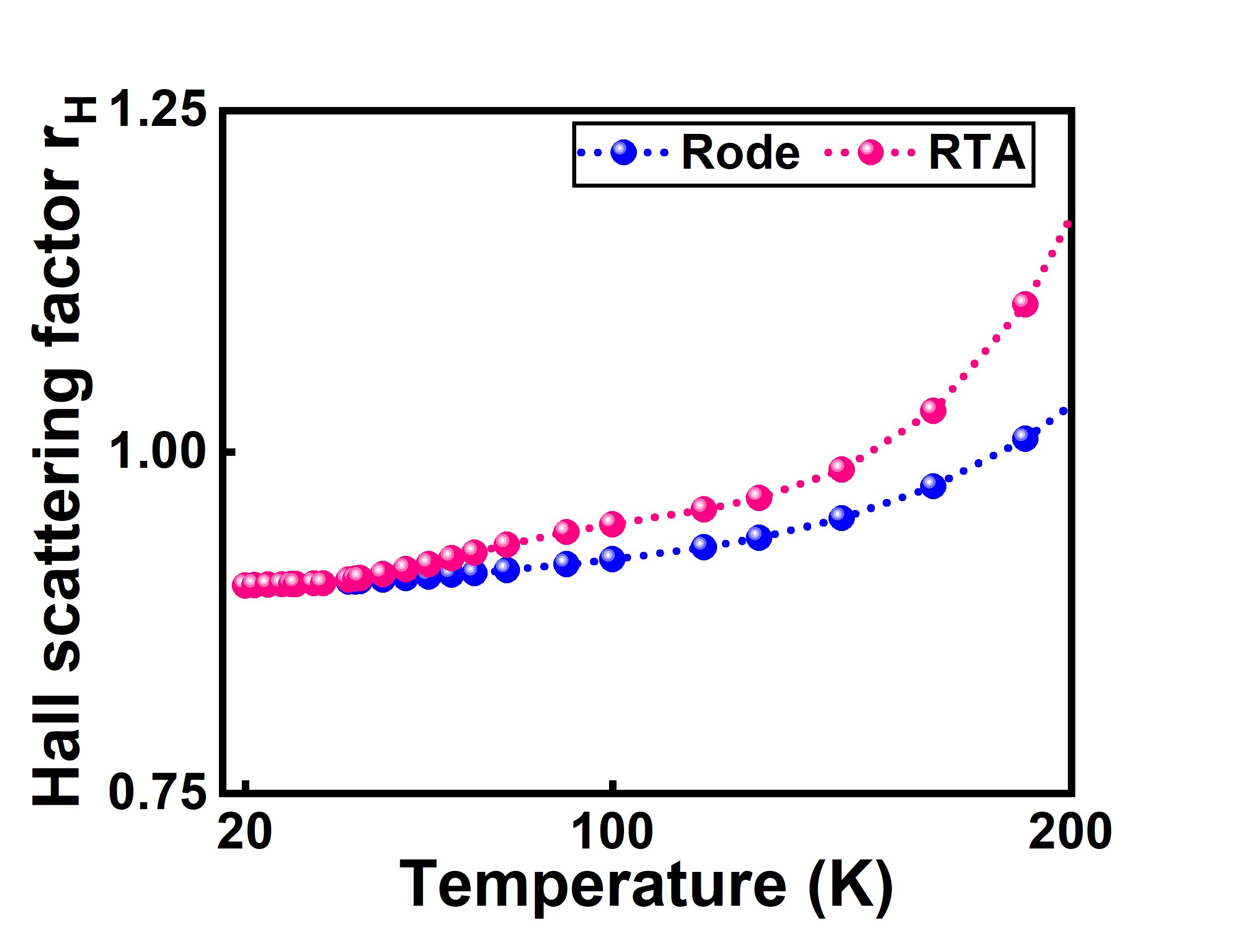
When the Hall scattering factor , deviates significantly from unity, it indicates that to derive the electron drift mobility from the experimentally calculated Hall mobility data, the Hall scattering factor must be precisely determined. Figure 13 shows the predicted values of the Hall scattering factor against the temperature at for , while Fig. 14 depicts the Hall scattering factor as a function of temperature and the carrier concentration at .
To the best of our knowledge, calculations of the Hall scattering factor in such SLs have not been performed yet in earlier works. The contribution of various scattering mechanisms decides the Hall scattering factor’s value. Figures 13 and 14 indicate that the value of at low temperatures deviates significantly from unity, while many researchers use one as an ideal value for a variety of calculations and studies, which is not accurate. The carrier concentration and the drift mobility may both be overestimated and underestimated when the Hall scattering factor is used as unity. The Hall scattering factor, in our calculation, fluctuates between the values as low as 0.3 at low temperature and electron concentration, and as high as 1.48 and even more at high temperature and electron concentration as shown in Fig. 14. Therefore, it is worth pointing out that, while evaluating the carrier concentration and the drift mobility in such SLs, one must use caution.
In this work, we calculate the precise values of the Hall scattering factor and show that for a doping value of , the computed values of are 0.914, 0.952 and 1.01 at temperatures of 77 K, 150 K and 190 K, respectively, as also depicted in Fig. 13. At higher temperatures, the value of the Hall scattering factor is more than unity, indicating that the drift mobility is lower than the Hall mobility, implying that the phonon-assisted scattering mechanisms are substantial and diminish the drift mobility. As shown in Fig. 14, at temperatures of 30 K and 77 K, the Hall scattering factor is equal to 0.335 & 0.638 for lower doping concentrations of and it is equal to 0.369 & 0.691 with slightly higher doping concentrations of which signifies that the Hall scattering factor increases as the temperature and electron concentrations rise, but as we increase the carrier concentration beyond , the Hall scattering factor starts decreasing. The higher electron concentration causes a rapid variation in the Hall factor.
V Conclusion
In this paper, we developed the Rode algorithm on the BTE in conjunction with the band structure and the EFA for a detailed computation of the carrier mobility and conductivity, in order to primarily unravel two crucial insights. First, the significance of both elastic and inelastic scattering mechanisms, particularly the influence of the IRS and POP scattering mechanisms in technologically relevant SL structures. Second, the structure specific Hall mobility and Hall scattering factor, which reveals that temperature and carrier concentrations significantly affect the Hall scattering factor, which deviates significantly from unity, i.e., from 0.3 to about 1.48, even for small magnetic fields. This reinforces the caution that should be exercised when employing the Hall scattering factor in experimental estimations of drift mobilities and carrier concentrations. Our research offers a comprehensive microscopic understanding of carrier dynamics in such technologically relevant SLs. Our model also provides highly accurate and precise transport parameters beyond the RTA and hence paves the way to develop physics based device modules for MWIR photodetectors.
Acknowledgments
The authors acknowledge funding from ISRO under the ISRO-IIT Bombay Space Technology Cell.
References
- Smith and Mailhiot (1987) D. Smith and C. Mailhiot, Journal of Applied Physics 62, 2545 (1987).
- Rogalski et al. (2017) A. Rogalski, P. Martyniuk, and M. Kopytko, Applied physics reviews 4, 031304 (2017).
- Mukherjee et al. (2021) S. Mukherjee, A. Singh, A. Bodhankar, and B. Muralidharan, Journal of Physics D: Applied Physics 54, 345104 (2021).
- Rogalski (2000) A. Rogalski, Infrared detectors (CRC press, 2000).
- Dehzangi et al. (2021) A. Dehzangi, J. Li, and M. Razeghi, Light: Science & Applications 10, 1 (2021).
- Rogalski (2003) A. Rogalski, Progress in quantum electronics 27, 59 (2003).
- Le Thi et al. (2019) Y. Le Thi, Y. Kamakura, and N. Mori, Japanese Journal of Applied Physics 58, 044002 (2019).
- Klipstein et al. (2021) P. Klipstein, Y. Benny, Y. Cohen, N. Fraenkel, R. Fraenkel, S. Gliksman, A. Glozman, I. Hirsch, O. Klin, L. Langof, et al., in Infrared Technology and Applications XLVII (SPIE, 2021), vol. 11741, pp. 102–112.
- Wróbel et al. (2012) J. Wróbel, P. Martyniuk, E. Plis, P. Madejczyk, W. Gawron, S. Krishna, and A. Rogalski, in Infrared Technology and Applications XXXVIII (SPIE, 2012), vol. 8353, pp. 412–420.
- Gautam et al. (2010) N. Gautam, H. Kim, M. Kutty, E. Plis, L. Dawson, and S. Krishna, Applied Physics Letters 96, 231107 (2010).
- Sai-Halasz et al. (1978) G. A. Sai-Halasz, L. Esaki, and W. A. Harrison, Phys. Rev. B 18, 2812 (1978).
- Manyk et al. (2018) T. Manyk, K. Michalczewski, K. Murawski, K. Grodecki, J. Rutkowski, and P. Martyniuk, Results in Physics 11, 1119 (2018).
- Rogalski et al. (2019) A. Rogalski, P. Martyniuk, and M. Kopytko, Progress in Quantum Electronics 68, 100228 (2019).
- Chow et al. (1991) D. Chow, R. Miles, J. Schulman, D. Collins, and T. McGill, Semiconductor Science and Technology 6, C47 (1991).
- Plis (2014) E. A. Plis, Advances in Electronics 2014 (2014).
- Martyniuk et al. (2014) P. Martyniuk, J. Antoszewski, M. Martyniuk, L. Faraone, and A. Rogalski, Applied Physics Reviews 1, 041102 (2014).
- Safa et al. (2013) S. Safa, A. Asgari, and L. Faraone, Journal of Applied Physics 114, 053712 (2013).
- Safa and Asgari (2015a) S. Safa and A. Asgari, arXiv preprint arXiv:1502.02449 (2015a).
- Safa and Asgari (2015b) S. Safa and A. Asgari, arXiv preprint arXiv:1502.01453 (2015b).
- Safa and Asgari (2015c) S. Safa and A. Asgari, arXiv preprint arXiv:1504.02871 (2015c).
- Szmulowicz et al. (2011) F. Szmulowicz, H. Haugan, S. Elhamri, and G. Brown, Physical Review B 84, 155307 (2011).
- Szmulowicz and Brown (2011) F. Szmulowicz and G. Brown, Applied Physics Letters 98, 182105 (2011).
- Szmulowicz and Brown (2013) F. Szmulowicz and G. Brown, Journal of Applied Physics 113, 014302 (2013).
- Bastard (1981) G. Bastard, Physical Review B 24, 5693 (1981).
- Conwell and Weisskopf (1950) E. Conwell and V. Weisskopf, Physical review 77, 388 (1950).
- Zook (1964) J. D. Zook, Physical Review 136, A869 (1964).
- Kaasbjerg et al. (2013) K. Kaasbjerg, K. S. Thygesen, and A.-P. Jauho, Physical Review B 87, 235312 (2013).
- Tsai et al. (2020) T.-Y. Tsai, K. Michalczewski, P. Martyniuk, C.-H. Wu, and Y.-R. Wu, Journal of Applied Physics 127, 033104 (2020).
- Wataya et al. (1989) M. Wataya, N. Sawaki, H. Goto, I. Akasaki, H. Kano, and M. Hashimoto, Japanese Journal of Applied Physics 28, 1934 (1989).
- Dharssi et al. (1991) I. Dharssi, P. Butcher, and G. Warren, Superlattices and microstructures 9, 335 (1991).
- Dharssi and Butcher (1990) I. Dharssi and P. Butcher, Journal of Physics: condensed matter 2, 4629 (1990).
- Rode (1970) D. Rode, Physical Review B 2, 1012 (1970).
- Rode (1973) D. Rode, physica status solidi (b) 55, 687 (1973).
- Rode (1975) D. Rode, in Semiconductors and semimetals (Elsevier, 1975), vol. 10, pp. 1–89.
- (35) N. W. Ashcroft, N. D. Mermin, et al., Solid state physics.
- Mermin (1970) N. D. Mermin, Physical Review B 1, 2362 (1970).
- Livneh et al. (2012) Y. Livneh, P. Klipstein, O. Klin, N. Snapi, S. Grossman, A. Glozman, and E. Weiss, Physical Review B 86, 235311 (2012).
- Klipstein (2010) P. Klipstein, Physical Review B 81, 235314 (2010).
- Ricciardi et al. (2020) C. Ricciardi, M. L. Della Rocca, and M. Benfante (2020).
- Qiao et al. (2012) P.-F. Qiao, S. Mou, and S. L. Chuang, Optics express 20, 2319 (2012).
- Klipstein et al. (2013) P. Klipstein, Y. Livneh, O. Klin, S. Grossman, N. Snapi, A. Glozman, and E. Weiss, Infrared Physics & Technology 59, 53 (2013).
- Aspnes and Studna (1983) D. E. Aspnes and A. Studna, Physical review B 27, 985 (1983).
- Datta (2005) S. Datta, Quantum transport: atom to transistor (Cambridge university press, 2005).
- Garwood et al. (2017) T. Garwood, N. A. Modine, and S. Krishna, Infrared Physics & Technology 81, 27 (2017).
- Wei and Razeghi (2004) Y. Wei and M. Razeghi, Physical Review B 69, 085316 (2004).
- Nucho and Madhukar (1978) R. Nucho and A. Madhukar, Journal of Vacuum Science and Technology 15, 1530 (1978).
- Dente and Tilton (1999) G. C. Dente and M. L. Tilton, Journal of Applied Physics 86, 1420 (1999).
- Magri and Zunger (2002) R. Magri and A. Zunger, Physical Review B 65, 165302 (2002).
- Taghipour et al. (2018) Z. Taghipour, E. Shojaee, and S. Krishna, Journal of Physics: Condensed Matter 30, 325701 (2018).
- Bastard (1982) G. Bastard, Physical Review B 25, 7584 (1982).
- Altarelli (1983) M. Altarelli, Physical review B 28, 842 (1983).
- Kane (1980) E. Kane, in Narrow Gap Semiconductors Physics and Applications (Springer, 1980), pp. 13–31.
- Chuang (2012) S. L. Chuang, Physics of photonic devices (John Wiley & Sons, 2012).
- Jiang et al. (2014) Y. Jiang, X. Ma, Y. Xu, and G. Song, Journal of Applied Physics 116, 173702 (2014).
- Dhar et al. (2013) N. K. Dhar, R. Dat, and A. K. Sood, Optoelectronics-Advanced Materials and Devices 1 (2013).
- Lundstrom (2002) M. Lundstrom, Fundamentals of carrier transport (2002).
- Ferry (2016) D. K. Ferry, Semiconductor transport (CRC Press, 2016).
- Singh (2007) J. Singh, Electronic and optoelectronic properties of semiconductor structures (Cambridge University Press, 2007).
- Pierret and Neudeck (1987) R. F. Pierret and G. W. Neudeck, Advanced semiconductor fundamentals, vol. 6 (Addison-Wesley Reading, MA, 1987).
- Vasileska et al. (2017) D. Vasileska, S. M. Goodnick, and G. Klimeck, Computational Electronics: semiclassical and quantum device modeling and simulation (CRC press, 2017).
- Chakrabarty et al. (2019) S. Chakrabarty, A. K. Mandia, B. Muralidharan, S. C. Lee, and S. Bhattacharjee, Journal of Physics: Condensed Matter 32, 135704 (2019).
- Mandia et al. (2021) A. K. Mandia, B. Muralidharan, J.-H. Choi, S.-C. Lee, and S. Bhattacharjee, Computer Physics Communications 259, 107697 (2021).
- Ganose et al. (2021) A. M. Ganose, J. Park, A. Faghaninia, R. Woods-Robinson, K. A. Persson, and A. Jain, Nature communications 12, 1 (2021).
- Brooks (1955) H. Brooks, in Advances in electronics and electron physics (Elsevier, 1955), vol. 7, pp. 85–182.
- Faghaninia et al. (2015) A. Faghaninia, J. W. Ager III, and C. S. Lo, Physical Review B 91, 235123 (2015).
- Kothari and Maldovan (2017) K. Kothari and M. Maldovan, Scientific Reports 7, 1 (2017).
- Sakaki et al. (1987) H. Sakaki, T. Noda, K. Hirakawa, M. Tanaka, and T. Matsusue, Applied physics letters 51, 1934 (1987).
- Gold (1987) A. Gold, Physical Review B 35, 723 (1987).
- Sang et al. (2013) L. Sang, S. Y. Yang, G. P. Liu, G. J. Zhao, C. B. Liu, C. Y. Gu, H. Y. Wei, X. L. Liu, Q. S. Zhu, and Z. G. Wang, IEEE transactions on electron devices 60, 2077 (2013).
- Goodnick et al. (1985) S. Goodnick, D. Ferry, C. Wilmsen, Z. Liliental, D. Fathy, and O. Krivanek, Physical Review B 32, 8171 (1985).
- Mandia et al. (2022) A. K. Mandia, N. A. Koshi, B. Muralidharan, S. C. Lee, and S. Bhattacharjee, Journal of Materials Chemistry C (2022).
- Becer et al. (2019) Z. Becer, A. Bennecer, and N. Sengouga, Crystals 9, 629 (2019).
- Vurgaftman et al. (2001) I. Vurgaftman, J. á. Meyer, and L. á. Ram-Mohan, Journal of applied physics 89, 5815 (2001).
- Delmas et al. (2019) M. Delmas, B. Liang, and D. L. Huffaker, in Quantum Sensing and Nano Electronics and Photonics XVI (International Society for Optics and Photonics, 2019), vol. 10926, p. 109260G.
- Mitra (1963) S. Mitra, Physical Review 132, 986 (1963).
- Lockwood et al. (2005) D. Lockwood, G. Yu, and N. Rowell, Solid State Communications 136, 404 (2005).
- Haugan et al. (2011) H. Haugan, G. Brown, F. Szmulowicz, and S. Elhamri, in AIP Conference Proceedings (American Institute of Physics, 2011), vol. 1416, pp. 155–157.
- Alchaar et al. (2019) R. Alchaar, J.-B. Rodriguez, L. Höglund, S. Naureen, and P. Christol, AIP Advances 9, 055012 (2019).