Advances toward high-accuracy gigahertz operation of tunable-barrier single-hole pumps in silicon
Abstract
Precise and reproducible current generation is key to realize quantum current standards in metrology. A promising candidate is a tunable-barrier single-charge pump, which can accurately transfer single charges one by one with an error rate of less than ppm level. Although several high-accuracy measurements have revealed such a high performance of the pumps, it is necessary to further pursue the possibility of high-precision operation toward reproducible generation of the pumping current in many devices. Here, we investigate in detail a silicon single-hole pumps, which are potentially expected to have a superior performance to single-electron pumps because of a heavy effective mass of holes. Temperature dependence measurements of current generated by the single-hole pump revealed a high energy selectivity of the tunnel barrier, which is a critical parameter to achieve high-accuracy operation. In addition, we applied the dynamic gate compensation technique to the single-hole pump and confirm the further performance improvement. Furthermore, we demonstrate gigahertz operation of a single-hole pump with an estimated lower bound of an error rate of around 0.01 ppm. These results imply a superior capability of single-hole pumps in silicon toward high-accuracy, high-speed, and stable single-charge pumping appropriate for not only metrological applications but also quantum device applications.
I Introduction
Single-charge pumping precisely controls a flow of single charges, enabling us to obtain a clean electric current. Among many potential applications including quantum information processing Bäuerle et al. (2018); Yamahata et al. (2019); Fletcher et al. (2023); Ubbelohde et al. (2023), single-photon sources Hsiao et al. (2020), and quantum sensing Johnson et al. (2017), a current standard application is a long-standing goal in the field of metrology Pekola et al. (2013). Toward this goal, high-accuracy pumping with an error rate of at least less than 0.1 ppm in the nanoampere regime is required. Precise evaluation of the accuracy began in earnest using a GaAs tunable-barrier single-electron (SE) pump about a decade ago Giblin et al. (2012). After that, many results demonstrating high precision of the tunable-barrier SE pumps were reported using GaAs Stein et al. (2015); Bae et al. (2015); Stein et al. (2017); Bae et al. (2020) and Si Yamahata et al. (2016); Zhao et al. (2017); Giblin et al. (2020, 2023) SE pumps, reaching an uncertainty of about 0.2 ppm. In terms of the current level, a nanoampere current was reported using trap-mediated pumping in Si Yamahata et al. (2014a, 2017) with increasing operating frequency at around 7 GHz. Parallelization of SE pumps is another important pathway to increase the current Maisi et al. (2009); Mirovsky et al. (2010); Kim et al. (2022). Note that there exist other approaches to obtain a current level in the nanoampere to milliampere regimes Brun-Picard et al. (2016); Shaikhaidarov et al. (2022); Rodenbach et al. (2023). In addition to the accuracy and current level, universality and reproducibility of devices are also important points. Universality of the pump was checked by investigating above many high-accuracy measurements Giblin et al. (2019). In terms of device reproducibility, our Si SE pumps so far show variability of the pumping accuracy Fujiwara et al. (2022). The reason of the spread is still under investigation but at least it is necessary to pursue capability of high-accuracy operation for the device to have reproducibility in terms of sub-ppm operation.
In general, the tunable-barrier SE pump in the tunneling regime at a low temperature can be accurately operated with a large charging energy of the quantum dot (QD) in the SE pump and a large energy selectivity of the entrance tunnel barrier characterized by an effective temperature Kaestner and Kashcheyevs (2015); Yamahata et al. (2014b). The former can be achieved by making a small QD and actually our Si devices have typically a large charging energy of about 10 - 20 meV Yamahata et al. (2011, 2019, 2023). An improvement would be necessary for the energy selectivity of the barrier. This can be achieved by making the barrier with a gentle curvature, which is related to a design of a gate electrode Fujiwara et al. (2022). Another way to enhance the energy selectivity is to use a charge carrier with a heavy effective mass. Since a hole is typically heavier than an electron in the case of Si Sze and Ng (2007), a single-hole (SH) pump is an attractive candidate for high-accuracy operation. We have previously reported gigahertz operation of SH pumping Yamahata et al. (2015) but it was high-temperature thermal-hopping regime and the accuracy was on the order of to . In addition, a Ge-based SH pump has recently been reported but the operating frequency was limited to 100 MHz and there was no discussion of the accuracy due to charge fluctuations Rossi et al. (2021). Therefore, further investigation about SH pumps is highly demanded.
Here, we investigate SH pumps in Si in the tunneling regime and show that the energy selectivity is much better than that in our previous investigation of an SE pump in Si Johnson et al. (2019). In addition, we applied gate compensation technique, which has been recently performed using GaAs pumps with two-gate high-frequency operation Hohls et al. (2022), and achieved enhancement of an estimated lower bound of a pumping error rate () from ppm to ppb levels. Furthermore, we demonstrate 2-GHz SH pumping with in a deep sub-ppm level.
II Device and measurement scheme
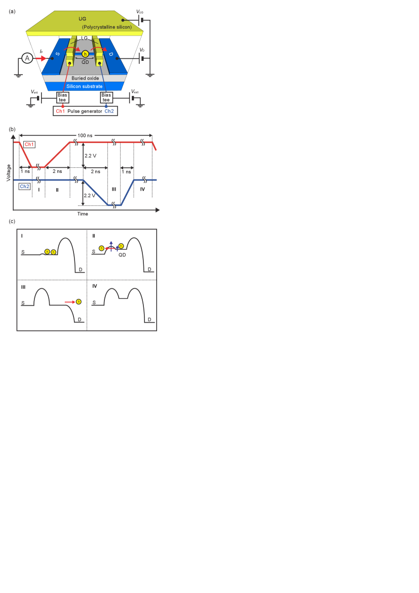
We fabricated a double-layer gate structure on a Si nanowire with a p-type source and drain [Fig. 1(a)]. The Si nanowire was patterned using electron beam lithography with dry etching, followed by thermal oxidation to form a gate insulator. The double-layer gate is made of an n-type polycrystalline Si grown by chemical vapor deposition. The upper and lower gates were patterned using electron beam lithograph and optical lithography, respectively, with dry etching. Interlayer oxide between the lower and upper gates was grown by thermal oxidation after the lower-gate formation. The source and drain were doped by boron atoms with ion implantation. The upper gate was used as a mask of the implantation. Aluminum ohmic contacts were finally formed by vacuum deposition. We measured two devices (devices A, B) for this study. The device sizes are summarized in Tab. 1. We show results of device A in Secs. III and IV and of device B in Sec. V.
We set device A in a dilution refrigerator with a base temperature of 50 mK. On the other hand, devices B was measured using a probe station with liquid helium at a stage temperature of around 4 K. For measurements of device A, we connected channels 1 and 2 in a pulse generator to the two lower gates with DC bias and , respectively. DC voltages and were also applied to the upper gate and drain, respectively. The DC current through the Si nanowire was measured at the source. For measurements of devices B, we used sinusoidal-signal generator instead of the channel 1 of the pulse generator and the channel 2 of the pulse generator was disconnected. Other connections were the same as those for device A.
Figure 1(b) schematically illustrates the outputs of the pulse generator. The frequency of the voltage pulses is 10 MHz. Note that the rise time of 2 ns in the channel 1 is roughly equivalent to 250-MHz operation with an application of a sinusoidal signal. For device A, we used turnstile operation to transfer SHs Fujiwara et al. (2004), in which sufficiently high drain bias was applied to have unidirectional transfer, because it can be easily extended to the gate compensation technique discussed in Sec. IV. The hole potential diagrams corresponding to regions I, II, III, and IV in Fig. 1(b) are shown in Fig. 1(c). In region I, some holes are loaded in the region between the two lower gates. In region II, the entrance barrier is raised. A QD is formed between the entrance and exit barriers. During this process, the QD potential is also raised because of the capacitive coupling between the entrance lower gate and QD. When the QD electrochemical potential exceeds the Fermi level of the source, some holes escape back to the source and finally an SH can be captured by the QD because the escape rate to the source eventually becomes negligibly slow. We refer to this process as a dynamic capture process and it was theoretically formulated using the decay cascade model Kashcheyevs and Kaestner (2010). After the rise of the entrance barrier, the exit barrier is lowered and it is the lowest in region III. During this process, the captured SH is ejected to the drain. Then, the exit barrier is raised but no additional SH is captured because of the large drain bias. When the number of the transferred SH is , the output current becomes , where is the elementally charge. For device B, the pulse voltage of the channel 1 is replaced to a sinusoidal signal. Without lowering exit barrier, a captured SH can be ejected to the drain because the QD potential becomes sufficiently high Fujiwara et al. (2008). The purpose of measurements of the device B is to check capability of high-frequency operation shown in Sec. V.
III High energy selectivity of tunnel barrier: device A
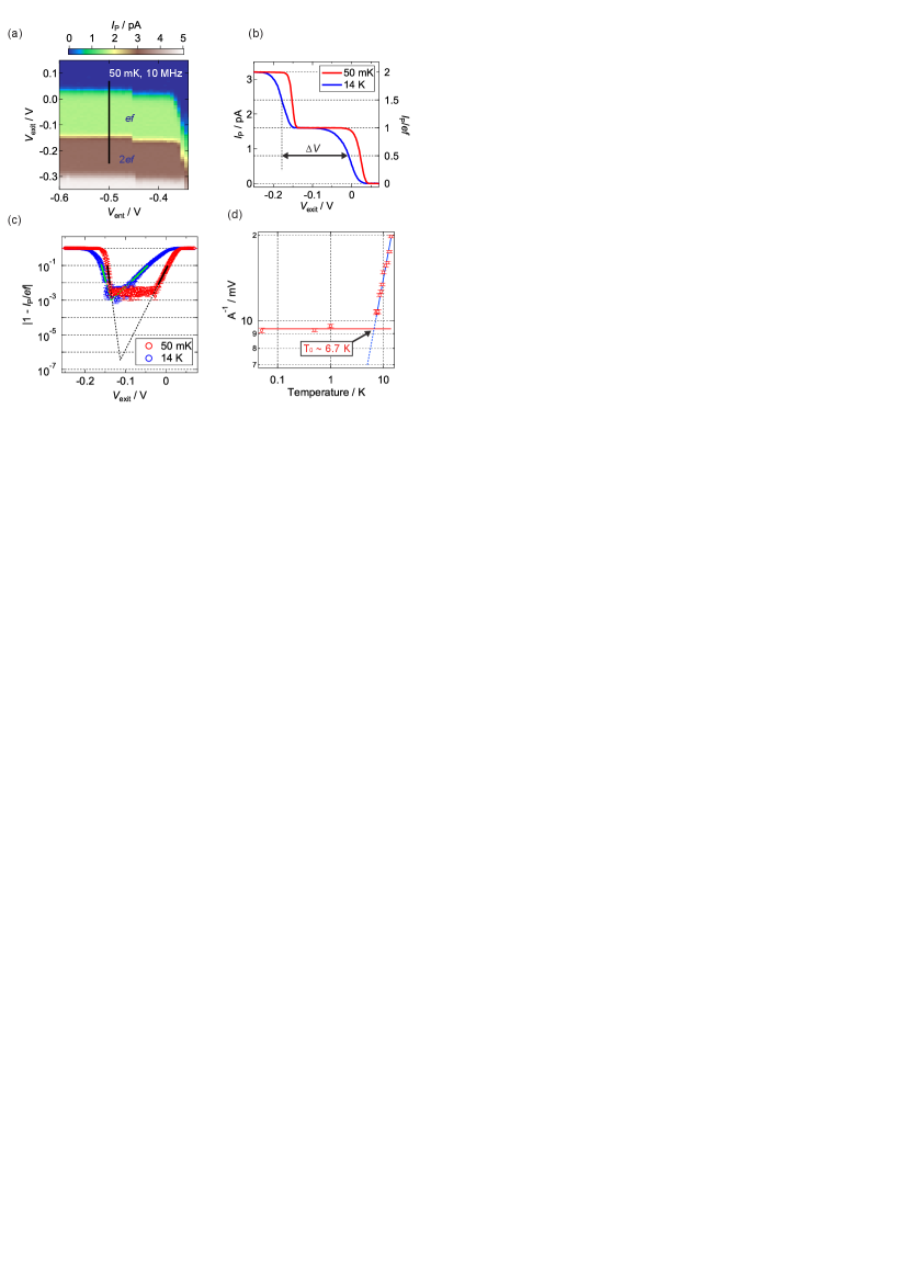
Figure 2(a) shows as a function of and for device A at 50 mK. along a black line in Fig. 2(a) is plotted as a red line in Fig. 2(b), where the current increase is determined by the dynamic capture process because of no dependence in Fig. 2(a). To evaluate the accuracy of the plateau, we plot [red circles in Fig. 2(c)], which indicates the relative deviation of the current plateau from an expected value of . Because of limitation of the measurement system, we measured the current with an uncertainty of the order of . From this kind of data, it is valuable to extract by extending exponential lines of the relative deviation Giblin et al. (2020); Yamahata et al. (2021). Although this method does not reveals a true accuracy of the pump and high-accuracy measurements are definitely necessary, it would be useful information because we can conveniently select a pump with a high possibility of high-accuracy operation and so far this extension looks reasonable on the sub-ppm level Giblin et al. (2023). A black line on the right in Fig. 2(c) is a fit to the data with a formula of [see Eq. (20)], where is the slope. A black line on the left in Fig. 2(c) is a phenomenological fit by a similar exponential function. We use extracted from the former fit in the following analysis. The intersection of two black dashed lines extending the two exponential fits indicates , which is about 0.69 ppm (twice the intersection value) in this specific device.
To more quantitatively understand , it is helpful to investigate a figure of merit parameter determining the pumping accuracy at a low temperature Kaestner and Kashcheyevs (2015); Yamahata et al. (2021), where is the charging energy of the QD, is the Boltzmann constant, and is a capacitive coupling parameter [see Eq. (5)]. Note that a typical value of our devices is on the order of 10 Fujiwara et al. (2022). To extract , we investigated temperature dependence of the inverse of the slope () because it is proportional to [see Eq. (15)] at a low temperature but at a high temperature it is proportional to . Therefore, the temperature at which begins to saturate corresponds to . A blue line in Fig. 2(b) and blue circles in Fig. 2(c) are and at 14 K, respectively. Similar to the 50-mK data, we fit the both side of and extract at the right side. Note that at 14 K is ppm. Figure 2(d) shows as a function of temperature. As expected, is constant in the low temperature regime but at around 10 K it linearly increases. A blue line in Fig. 2(d) is a linear fit to . A red horizontal line is a mean value of the low temperature data at 1, 0.5, and 0.05 K. We estimate from the intersection point between the extension of the blue line (blue dashed line) and the red line, resulting in K. We additionally evaluate from the 14-K data shown in Fig. 2(b). From the value of and the spacing of plateau of about 170 mV, we extract meV. This value is similar to that of the previous SH pump ( meV) Yamahata et al. (2015). From the extracted values, we obtain of about at a low temperature.
In the previous estimation of our Si SE pump Johnson et al. (2019), meV and K. Although charging energy was larger in this case, the large leads to . This indicates that the low in the SH pump leads to the good characteristics. Theoretically, it is likely to be attributed to the difference of the effective mass between electron (: typically, ) and hole (: typically, ), where is the bare electron mass Sze and Ng (2007); Yamahata et al. (2015). Assuming a parabolic potential barrier characterized by , barrier curvature at is . Therefore, . In this case, Yamahata et al. (2014b). Therefore, of a hole could be times larger than that of an electron. When is independent of the effective mass (i.e., a self capacitance dominates Yamahata et al. (2011)), this directly leads to the enhancement of of about 1.6. This enhancement corresponds to more than two order magnitude enhancement of .
IV Dynamic gate compensation: device A
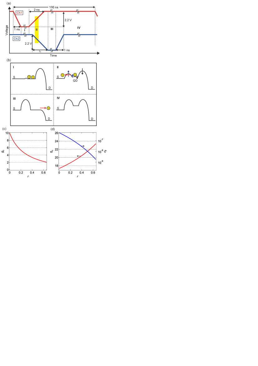
ppm of device A is a relatively good value but is not sufficient for the metrological applications. Here, we use dynamic gate compensation technique proposed in Ref. Hohls et al. (2022) to the Si SH pump to show the universality of the technique and potential of our device. The concept of the compensation is to suppress the change in the potential of the QD in the dynamic capture process by additionally changing the signal applied to the exit gate. In our case, we changed the delay time of the voltage pulses in the channel 2 to match the voltage rise in the channel 1 with the voltage fall with a time duration of in the channel 2 [Fig. 3(a)]. At region II, the QD potential is additionally lowered by the signal applied to the exit gate [Fig. 3(b)]. This leads to the change in the dynamic capture probability.
Following the method described in Ref. Yamahata et al. (2021), we include the compensation effect to the dynamic capture probability as
| (1) |
where is the ratio of the slopes of the high-frequency signals applied to the entrance and exit gates (see Appendix A), is defined as Eq. (18), and is the effective capacitive coupling parameter with the compensation effect given as Eq. (6). In addition, a figure of merit parameter determining the accuracy of the dynamic capture can be written as (see Appendix A),
| (2) |
Since decreases with increasing [Fig. 3(c)], (i.e., ) increases (decreases) with increasing [Fig. 3(d)]. Note that these discussions are identical to what were discussed in Ref. Hohls et al. (2022) but our purpose here is to clearly show a relation between the compensation technique to the discussion of the effect of describing in Ref. Yamahata et al. (2021), which would helps understanding of the mechanism of the compensation effect.
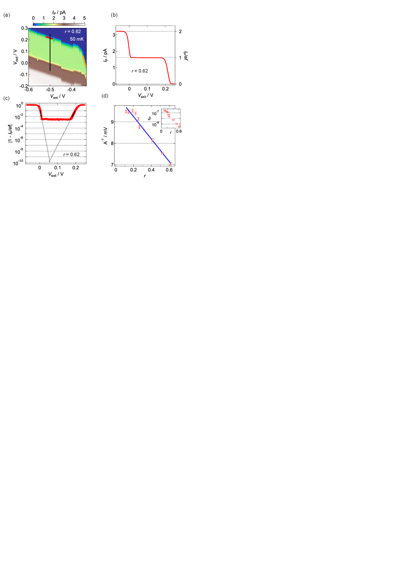
We measured at ns as a function of and [Fig. 4(a)]. Since the slope of the line with the same current level dominated by the dynamic capture process determines only by [see Eq. (1)], we perform a linear fit to the line [red line in Fig. 4(a)], resulting in of 0.62. The current plateau along a black line in Fig. 4(a) is plotted in Fig. 4(b). Figure 4(c) is for this case. Similar to Fig. 2(c), we extracted the slope of the current and plot the inverse of the slope as a function of extracted from pumping current maps [Fig. 4(d)]. Note that was changed by changing . A blue line in Fig. 4(d) is a fit to using Eq. (18), yielding eV/V and eV/V, where , and and are the voltage-to-energy conversion factors between the entrance gate and entrance barrier and between the exit gate and QD, respectively. This good fit indicates effectiveness of the gate compensation technique. Note that slight fluctuation of the value of the slope could be related to potential fluctuation in the QD. We also extracted by extending the exponential fits in Fig. 4(c). With increasing , decreases from ppm to ppb levels [inset in Fig. 4(d)], which roughly corresponds to the simplified expectation shown in Fig. 3(d) [the extracted conversion factors are used in Figs. 3(c) and (d)]. This accuracy level is sufficient for the metrological application.
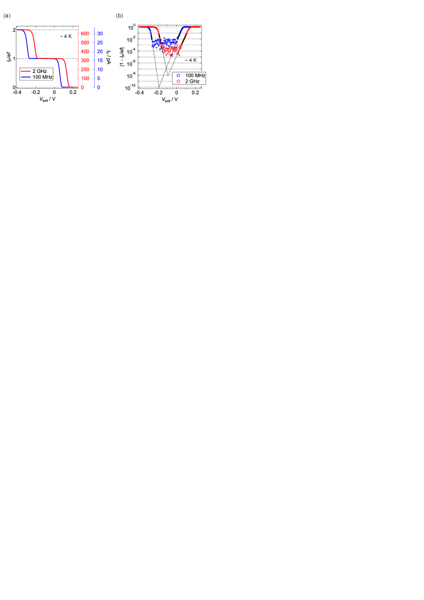
V Gigahertz operation: device B
In another device, we measured frequency dependence of the current plateau of the SH pumping. Figure 5(a) shows as a function of for device B at 100 MHz and 2 GHz at around 4 K. Corresponding is plotted in Fig. 5(b). Similar to the above analysis, we perform an exponential fit to the data and extract . In this specific device, the error rate is on the order of 0.01 ppm for the 2-GHz operation. This also indicates potential of the SH pumping. We also observe the increase in with increasing frequency. This is a general trend of single-charge pumps Giblin et al. (2012); Seo et al. (2014); Yamahata et al. (2015, 2016) possibly due to nonadiabatic excitation of a hole confined in the QD suring the dynamic QD movement Kataoka et al. (2011) and it should be further investigated in future works.
VI Conclusions
We have observed a high energy selectivity of the entrance barrier (low ) of a Si SH pump. This superior property is important for the high-accuracy operation with high yield. By using the gate compensation technique, we confirmed that the pump performance was further improved to the level suitable for the metrological application. Furthermore, we have demonstrated 2-GHz SH pumping in another SH pump with an estimated lower bound of error rate of about 0.01 ppm. These results would indicate high potential of SH pumps. In future work, it is necessary to check variability of among many devices with an identical design. In addition, pumping characteristics of an SH and SE should be compared with the same QD by making N-type and P-type ohmic contacts simultaneously Noborisaka et al. (2014).
Acknowledgements.
We thank T. Shimizu, F. Hohls, and V. Kashcheyevs for fruitful discussions. This work was partly supported by JSPS KAKENHI Grant Number JP18H05258.Data availability
The data that support the findings of the study are available from the corresponding author upon reasonable request.
Appendix A Formulation of dynamic gate compensation
We formulate the gate-compensation effect for an SH pumping [region II in Fig. 3(a)] using a capacitive coupling parameter and its extended version following the method described in Ref. Yamahata et al. (2021). For simplicity, we use the constant interaction model Kouwenhoven et al. (2001); van der Wiel et al. (2003) with a single level. In this case, the potential energy of the QD with one electron and the height of the entrance barrier can be calculated as
| (3) | ||||
| (4) |
respectively, where we set and when , is the charging energy of the QD, and are voltage-to-energy conversion factors between the entrance (exit) gate and QD and between the entrance (exit) gate and entrance barrier, respectively, we assume a linear ramp of the voltage pulses with a coefficient of , and is the ratio of the slopes of the voltage pulses at the entrance gate to that of the exit gates. Note that the signs preceding the voltage-to-energy conversion factors are positive because our focus is an SH pumping. The parameter () is defined as a ratio between the QD potential change and the change in the barrier height with respect to the QD potential during the rise of the entrance barrier without (with) the compensation, given as
| (5) | ||||
| (6) |
Then, the tunnel rate of a hole between the QD and source is calculated as
| (7) | ||||
| (8) |
where
| (9) | ||||
| (10) |
and is a constant. Note that is replaced with in the high-temperature thermal-hopping regime. A time when the detailed balance breaks down is defined as , leading to . Then, we obtain
| (11) |
This equation is equivalent to Eq. (14) of Ref. Yamahata et al. (2021) when (no compensation). The SH dynamics is governed by the master equation [Eqs. (4)-(6) in Ref. Yamahata et al. (2021)] and the steady state is expressed as [see Eqs. (8) and (13) in Ref. Yamahata et al. (2021)]
| (12) | ||||
| (13) |
where is the Fermi function, we use the relation of , and . From this equation, the probability distribution for the decay cascade model can be calculated as [see Eq. (16) in Ref. Yamahata et al. (2021)]
| (14) | ||||
| (15) |
where
| (16) | ||||
| (17) | ||||
| (18) |
and . Equation (17) is identical to geometrically derived Eq. (4) in Ref. Hohls et al. (2022). For the fit to in Fig. 4(d), we used Eq. (18). For estimation of , we used the slope of the loading process [region I in Fig. 3(a)] indicated by an orange line in Fig. 4(a). Since this loading process is dominated by the entrance barrier height, Yamahata et al. (2019). The orange line in Fig. 4(a) is a linear fit to a contour line with a current level of 1 pA, yielding . For the evaluation of , we calculate as
| (19) | ||||
| (20) |
where we assume that . Furthermore, since Eq. (15) is identical to Eq. (16) in Ref. Yamahata et al. (2021) when is replaced to , a figure of merit parameter when the compensation is applied can be written as [see Eq. (20) in Ref. Yamahata et al. (2021)]
| (21) |
References
- Bäuerle et al. (2018) C. Bäuerle, D. C. Glattli, T. Meunier, F. Portier, P. Roche, P. Roulleau, S. Takada, and X. Waintal, Rep. Prog. Phys. 81, 056503 (2018).
- Yamahata et al. (2019) G. Yamahata, S. Ryu, N. Johnson, H. -S. Sim, A. Fujiwara, and M. Kataoka, Nat. Nanotechnol. 14, 1019 (2019).
- Fletcher et al. (2023) J. Fletcher, W. Park, S. Ryu, P. See, J. P. Griffiths, G. A. C. Jones, I. Farrer, D. A. Ritchie, H. -S. Sim, and M. Kataoka, Nat. Nanotechnol. 18, 727 (2023).
- Ubbelohde et al. (2023) N. Ubbelohde, L. Freise, E. Pavlovska, P. G. Silvestrov, P. Recher, M. Kokainis, G. Barinovs, F. Hohls, T. Weimann, K. Pierz, and V. Kashcheyevs, Nat. Nanotechnol. 18, 733 (2023).
- Hsiao et al. (2020) T. -K. Hsiao, A. Rubino, Y. Chung, S. -K. Son, H. Hou, J. Pedrós, A. Nasir, G. Éthier-Majcher, M. J. Stanley, R. T. Phillips, T. A. Mitchell, J. P. Griffiths, I. Farrer, D. A. Ritchie, and C. J. B. Ford, Nat. Commun. 11, 917 (2020).
- Johnson et al. (2017) N. Johnson, J. D. Fletcher, D. A. Humphreys, P. See, J. P. Griffiths, G. A. C. Jones, I. Farrer, D. A. Ritchie, M. Pepper, T. J. B. M. Janssen, and M. Kataoka, Appl. Phys. Lett. 110, 102105 (2017).
- Pekola et al. (2013) J. P. Pekola, O. -P. Saira, V. F. Maisi, A. Kemppinen, M. Möttönen, Y. A. Pashkin, and D. V. Averin, Rev. Mod. Phys. 85, 1421 (2013).
- Giblin et al. (2012) S. P. Giblin, M. Kataoka, J. D. Fletcher, P. See, T. J. B. M. Janssen, J. P. Griffiths, G. A. C. Jones, I. Farrer, and D. A. Ritchie, Nat. Commun. 3, 930 (2012).
- Stein et al. (2015) F. Stein, D. Drung, L. Fricke, H. Scherer, F. Hohls, C. Leicht, M. Götz, C. Krause, R. Behr, E. Pesel, K. Pierz, U. Siegner, F. J. Ahlers, and H. W. Schumacher, Appl. Phys. Lett. 107, 103501 (2015).
- Bae et al. (2015) M. -H. Bae, Y. -H. Ahn, M. Seo, Y. Chung, J. D. Fletcher, S. P. Giblin, M. Kataoka, and N. Kim, Metrologia 52, 195 (2015).
- Stein et al. (2017) F. Stein, H. Scherer, T. Gerster, R. Behr, M. Götz, E. Pesel, C. Leicht, N. Ubbelohde, T. Weimann, K. Pierz, H. W. Schumacher, and F. Hohls, Metrologia 54, S1 (2017).
- Bae et al. (2020) M. -H. Bae, D. -H. Chae, M. -S. Kim, B. -K. Kim, S. -I. Park, J. Song, T. Oe, N. -H. Kaneko, N. Kim, and W. -S. Kim, Metrologia 57, 065025 (2020).
- Yamahata et al. (2016) G. Yamahata, S. P. Giblin, M. Kataoka, T. Karasawa, and A. Fujiwara, Appl. Phys. Lett. 109, 013101 (2016).
- Zhao et al. (2017) R. Zhao, A. Rossi, S. P. Giblin, J. D. Fletcher, F. E. Hudson, M. Möttönen, M. Kataoka, and A. S. Dzurak, Phys. Rev. Appl. 8, 044021 (2017).
- Giblin et al. (2020) S. P. Giblin, E. Mykkänen, A. Kemppinen, P. Immonen, A. Manninen, M. Jenei, M. Möttönen, G. Yamahata, A. Fujiwara, and M. Kataoka, Metrologia 57, 025013 (2020).
- Giblin et al. (2023) S. P. Giblin, G. Yamahata, A. Fujiwara, and M. Kataoka, Metrologia 60, 055001 (2023).
- Yamahata et al. (2014a) G. Yamahata, K. Nishiguchi, and A. Fujiwara, Nat. Commun. 5, 5038 (2014a).
- Yamahata et al. (2017) G. Yamahata, S. P. Giblin, M. Kataoka, T. Karasawa, and A. Fujiwara, Sci. Rep. 7, 45137 (2017).
- Maisi et al. (2009) V. F. Maisi, Y. A. Pashkin, S. Kafanov, J. -S. Tsai, and J. P. Pekola, New J. Phys. 11, 113057 (2009).
- Mirovsky et al. (2010) P. Mirovsky, B. Kaestner, C. Leicht, A. C. Welker, T. Weimann, K. Pierz, and H. W. Schumacher, Appl. Phys. Lett. 97, 252104 (2010).
- Kim et al. (2022) B. -K. Kim, B. -S. Yu, S. -I. Park, J. Song, N. Kim, and M. -H. Bae, AIP Advances 12, 105118 (2022).
- Brun-Picard et al. (2016) J. Brun-Picard, S. Djordjevic, D. Leprat, F. Schopfer, and W. Poirier, Phys. Rev. X 6, 041051 (2016).
- Shaikhaidarov et al. (2022) R. S. Shaikhaidarov, K. H. Kim, J. W. Dunstan, I. V. Antonov, S. Linzen, M. Ziegler, D. S. Golubev, V. N. Antonov, E. V. Il’ichev, and O. V. Astafiev, Nature 608, 45 (2022).
- Rodenbach et al. (2023) L. K. Rodenbach, N. T. M. Tran, J. M. Underwood, A. R. Panna, M. P. Andersen, Z. S. Barcikowski, S. U. Payagala, P. Zhang, L. Tai, K. L. Wang, R. E. Elmquist, D. G. Jarrett, D. B. Newell, A. F. Rigosi, and D. Goldhaber-Gordon, arXiv:2308.00200 (2023).
- Giblin et al. (2019) S. P. Giblin, A. Fujiwara, G. Yamahata, M. -H. Bae, N. Kim, A. Rossi, M. Möttönen, and M. Kataoka, Metrologia 56, 044004 (2019).
- Fujiwara et al. (2022) A. Fujiwara, G. Yamahata, and N. Johnson, Conference on Precision Electromagnetic Measurements (CPEM 2022) (2022).
- Kaestner and Kashcheyevs (2015) B. Kaestner and V. Kashcheyevs, Rep. Prog. Phys. 78, 103901 (2015).
- Yamahata et al. (2014b) G. Yamahata, K. Nishiguchi, and A. Fujiwara, Phys. Rev. B 89, 165302 (2014b).
- Yamahata et al. (2011) G. Yamahata, K. Nishiguchi, and A. Fujiwara, Appl. Phys. Lett. 98, 222104 (2011).
- Yamahata et al. (2023) G. Yamahata, N. Johnson, and A. Fujiwara, arXiv:2303.17242. (2023).
- Sze and Ng (2007) S. M. Sze and K. K. Ng, Physics of Semiconductor Devices, 3rd ed. (John Wiley & Sons, 2007).
- Yamahata et al. (2015) G. Yamahata, T. Karasawa, and A. Fujiwara, Appl. Phys. Lett. 106, 023112 (2015).
- Rossi et al. (2021) A. Rossi, N. W. Hendrickx, A. Sammak, M. Veldhorst, G. Scappucci, and M. Kataoka, J. Phys. D: Appl. Phys 54, 434001 (2021).
- Johnson et al. (2019) N. Johnson, G. Yamahata, and A. Fujiwara, Appl. Phys. Lett. 115, 162103 (2019).
- Hohls et al. (2022) F. Hohls, V. Kashcheyevs, F. Stein, T. Wenz, B. Kaestner, and H. W. Schumacher, Phys. Rev. B 105, 205425 (2022).
- Fujiwara et al. (2004) A. Fujiwara, N. M. Zimmerman, Y. Ono, and Y. Takahashi, Appl. Phys. Lett. 84, 1323 (2004).
- Kashcheyevs and Kaestner (2010) V. Kashcheyevs and B. Kaestner, Phys. Rev. Lett. 104, 186805 (2010).
- Fujiwara et al. (2008) A. Fujiwara, K. Nishiguchi, and Y. Ono, Appl. Phys. Lett. 92, 042102 (2008).
- Yamahata et al. (2021) G. Yamahata, N. Johnson, and A. Fujiwara, Phys. Rev. B 103, 245306 (2021).
- Seo et al. (2014) M. Seo, Y. -H. Ahn, Y. Oh, Y. Chung, S. Ryu, H. -S. Sim, I. -H. Lee, M. -H. Bae, and N. Kim, Phys. Rev. B 90, 085307 (2014).
- Kataoka et al. (2011) M. Kataoka, J. D. Fletcher, P. See, S. P. Giblin, T. J. B. M. Janssen, J. P. Griffiths, G. A. C. Jones, I. Farrer, and D. A. Ritchie, Phys. Rev. Lett. 106, 126801 (2011).
- Noborisaka et al. (2014) J. Noborisaka, K. Nishiguchi, and A. Fujiwara, Sci. Rep. 4, 6950 (2014).
- Kouwenhoven et al. (2001) L. P. Kouwenhoven, D. G. Austing, and S. Tarucha, Rep. Prog. Phys 64, 701 (2001).
- van der Wiel et al. (2003) W. G. van der Wiel, S. D. Franceschi, J. M. Elzerman, T. Fujisawa, S. Tarucha, and L. P. Kouwenhoven, Rev. Mod. Phys 75, 1 (2003).
- Fujiwara et al. (2016) A. Fujiwara, G. Yamahata, and K. Nishiguchi, Nanoscale Silicon Devices (Boca Raton, FL: CRC Press, 2016) Chap. 9, p. 207.
| Device | Wire thickness | Wire width | Gate space | Gate length |
|---|---|---|---|---|
| A | 15 nm | 20 nm | 80 nm | 40 nm |
| B | 15 nm | 20 nm | 80 nm | 10 nm |