Abrupt degenerately-doped silicon nanowire tunnel junctions
Abstract
We have confirmed the presence of narrow, degenerately-doped axial silicon nanowire (SiNW) p-n junctions via off-axis electron holography (EH). SiNWs were grown via the vapor-solid-liquid (VLS) mechanism using gold (Au) as the catalyst, silane (SiH4), diborane (B2H6) and phosphine (PH3) as the precursors, and hydrochloric acid (HCl) to stabilize the growth. Two types of growth were carried out, and in each case we explored growth with both n/p and p/n sequences. In the first type, we abruptly switched the dopant precursors at the desired junction location, and in the second type we slowed the growth rate at the junction to allow the dopants to readily leave the Au catalyst. We demonstrate degenerately-doped p/n and n/p nanowire segments with abrupt potential profiles of and V, and depletion region widths as narrow as nm via EH. Low temperature current-voltage measurements show an asymmetric curvature in the forward direction that resemble planar gold-doped tunnel junctions, where the tunneling current is hidden by a large excess current. The results presented herein show that the direct VLS growth of degenerately-doped axial SiNW p-n junctions is feasible, an essential step in the fabrication of more complex SiNW-based devices for electronics and solar energy.
pacs:
11ams:
44Keywords: Silicon nanowires, tunnel junctions, off-axis electron holography
1 Introduction
Silicon (Si) continues to hold a prevalent position at the heart of solar energy conversion and the microelectronics industry. Its abundance, non-toxicity and excellent photoelectric behavior have not only made Si ubiquitous in these fields but have also encouraged the development of technologies for its extraction and processing, making it very competitive in terms of clean energy production [1, 2, 3]. Silicon nanowires (SiNWs) are especially attractive for a variety of applications that benefit from the large surface-area-to-volume ratio of this pseudo 1-dimensional geometry, including sensors [4, 5, 6], electrodes [7, 8], and energy harvesters [9].
One type of electronic junction that is a challenge to fabricate, especially for nanowires (NWs) created via vapor-liquid-solid (VLS) growth mechanisms, is the tunnel (Esaki) diode. In the simplest case, these are homo-junctions consisting of abrupt transitions between degenerately-doped p and n-type segments of the same semiconductor. Narrow depletions regions, less than 10 nm are optimal, allowing carriers to tunnel through the potential energy barrier at low applied biases [10]. The ideal current-voltage (I-V) characteristics show an interesting negative-differential resistance (NDR) curve. Lattice-mismatched NW heterojunctions, including InP/Si [11], InP/GaAs [12], InP/GaInP [13] and GaSb/InAs [14, 15, 16] have been reported to form tunnel junctions. The latter exploited a type II band alignment that can enhance tunneling probabilities without further doping.
Many factors impede the formation of the perfect structure. A catalyst reservoir effect may broaden the width of the depletion region by prolonging the release of a dopant precursor after the vapor-phase sources are turned off and/or switched [11, 12, 17]. The limited solubility of different precursors at characteristic VLS growth temperatures can hinder the ability to reach degenerate-doping profiles [18]. Other challenges are related to catalyst segregation, unwanted stacking faults, kinking and radial growth, and the formation of undesired radial junctions in addition to the axial junction.
SiNW growth using silane (SiH4) as the Si source and phosphine (PH3) and diborane (B2H6) as the n- and p-type dopant precursors, respectively, is well established [19, 20, 21, 22, 17]. It is possible to suppress the reservoir effect to form very abrupt degenerately-doped n-type-to-intrinsic transitions by choosing growth conditions in which the P evaporation (associative desorption) greatly dominates over crystallization at the liquid-solid interface [23, 17]. However, growth of degenerately-doped p-type SiNWs (B-doped) has been challenging and has impeded the creation of a SiNW tunnel junction except where a degenerate p-type doped Si substrate is used[18]. While higher temperatures aid the uniformity of radial dopant distributions, this also increases the decomposition rate of the SiH4 precursor, creating a non-selective vapor-solid (VS) Si shell growth on the NW sidewalls [24]. Diborane also catalyzes the decomposition SiH4, intensifying the p-type growth problems [19]. Sidewall deposition can be eliminated by adding hydrochloric acid (HCl), which is known to create monochlorinated surface species that passivate surfaces and act as a barrier to deposition. Using HCl passivation and lower growth temperatures, degenerate doping above the thermodynamic solubility limit has recently been achieved in p-type SiNWs with no evident VS deposition on the sidewalls [19] allowing for the growth of p-n SiNW superlattices.
Evaluation of the depletion region width in a NW p-n junction can be carried out through various methods, including wet chemical etching [25], secondary electron (SE) imaging [26, 27], off-axis electron holography (EH) [28, 29, 30, 31], electron beam induced current (EBIC) [32, 33], Kelvin probe force microscopy [34, 35], and other AFM-based techniques such as scanning capacitance microscopy (SCM) [36, 37] and scattering-type scanning near-field optical microscopy [38]. Methods based on secondary ion mass spectroscopy including atom probe tomography are very powerful at mapping dopants [39], but they cannot evaluate the level of activation in the dopant impurities detected. Wet chemical etching, SE imaging and EBIC provide spatial junction profile information but are unable to evaluate junction potential directly, and AFM techniques often require additional information to separate surface from bulk potentials. EH is a transmission electron microscopy (TEM) technique that provides two dimensional maps of the average built-in potential of a p-n junction with a resolution 5 nm. It is becoming increasingly used in the characterization of NWs, [40, 29, 41, 42] including SiNWs [31, 30, 43].
The phase change of an electron wave after passing through a non-magnetic specimen of thickness is given by
| (1) |
for low dynamical scattering conditions, away from strong diffraction. Here, is an electron-energy-dependent interaction constant ( rads at 200 keV), is the direction of the electron beam, and is the electrostatic potential which includes the periodic potential of the crystal, known as the mean inner potential (MIP), the built-in junction potential () of the space charge region, and other possible potentials arising from charge accumulation induced by the electron beam. NWs are usually the perfect candidates for EH, because they are highly symmetric and require no chemical or mechanical thinning to become electron transparent. If the NW is grounded to the grid, then the degenerately-doped junction is assumed to be unbiased and the chemical potential (i.e. the Fermi level) will be independent of position across the junction. The potential drop at a degenerately-doped p-n junction is approximately the value of the bandgap.
EH has been used to image lateral gradients in GaP core-shell NW p-n junctions and to assess the efficiency of dopant incorporation [28]. It was also used to measure the abruptness of an axial, degenerately-doped, GaAs NW homojunction finding a depletion width of nm with a junction potential comparable to the bandgap, eV. A small diameter reduction in the NW occurring before the p-n junction formation also lead to the conclusion that there was a delay in the diethylzinc (DEZn) incorporation [29]. Gan et al. mapped the electrostatic potential across axial SiNWs p-n junctions through EH, finding a junction height of V, with a Schottky barrier at the Au metal contact of [31]. The profiles in SiNWs junctions have been interpreted to have a doping profile abruptness of less than 30 nm/decade[30].
In this paper, SiNWs were grown via HCl-stabilized VLS growth with Au catalysts onto thermally-oxidized (300 nm) Si (001) wafers. Two growth sequences, n/p and p/n, with degenerate-doping levels were synthesized. The effect of the precursor gas flow process and growth rate at the junction regions on SiNW properties were investigated towards reduction of Au segregation and improvement in dopant incorporation and abruptness. We used EH to map the and junction depletion width. Depletion regions as short as nm and values that are comparable to the Si bandgap were measured. Low temperature I-V measurements showed an effective low-bias resistance as low as and a slope change in the forward-bias direction characteristic of Au-doped p-n tunnel junctions.
Results
Figure 1 shows gas flow schemes for the two growth processes that were compared for each sequence: n/p and p/n. In the standard process (Growth 1), the flow rate of the Si gas flow (SiH4) was unchanged while the dopant-precursor flows were abruptly changed at the junction location. In the modified growth process (Growth 2), the SiH4 flow rate was reduced from the standard rate by an order of magnitude, to reduce the growth rate, before the junction region, and then increased back to the original flow rates after the junction. The flow rate of the dopant precursors, was also reduced to maintain the same Si:dopant ratio. Growth 2 was designed to test if slowing the NW growth rate and allowing more time for dopant atoms to evaporate from the catalyst would facilitate an increase in junction abruptness [17, 19, 21, 44].

Figure 2 shows a SE image via focused helium ion microscopy (HIM) and a bright-field TEM image of representative NWs resulting from Growth 1 in the p/n sequence. Images of SiNWs from other growths did not vary from these results, except for the presence of kinks nearby the junction, more commonly observed for NWs of Growth 2. In both Figure 2(a) and (b) the Au catalyst particle is visible at the right end. The length of the SiNWs typically varied from 12 to 18 m with the p-n junction expected at 1.4 to 1.7 m from the Au catalyst end. The HIM SE image shows strong contrast at the lateral edges of each NW typical for this technique. There is a reduction in intensity near holes in the support grid related to transmission of the He ion beam through the sample. Although experimental parameters such as magnification, ion beam energy and working distance were chosen to maximize SE contrast, there was no sign of a p-n junction. The native oxide developed by these SiNWs is shown in the TEM image detail in Figure 2(c). Similar to SEM imaging of p-n junctions, the likely presence of mid-gap interface states at the oxide interface probably leveled any difference in the SE emission rates between the n and p-type segments, masking the dopant transition. In Figure 2(b) the bright-field TEM contrast is primarily due to variations in the intensity of diffraction. The thin black line in the upper part of the NW corresponds to another much smaller SiNW that adhered during TEM sample preparation. Other TEM studies showing the development of a twin boundary bisecting some of these NWs [39] can be found in the Supplemental Information.

Figure 3 shows representative EH results for SiNWs resulting from Growth 1, in both the p/n and n/p growth sequences. The contrast seen in the bright-field TEM image in Figure 3(c) is rather uniform and due entirely to differences in the degree of diffraction from small angle bending and thickness variations, except for small dark spots that accumulated at the junction area indicative of a higher atomic number element (e.g. Au). Also, note the smaller SiNW in Figure 3(c), that seems to have nucleated on a particle located close by the junction. In Figure 3(d), we see strong contrast from stacking fault defects nearby the junction area. This type of defect developed independently of growth sequence or doping type and was randomly distributed along most NWs. Figure 3(e) and (f) show a reconstructed phase map with respect to the vacuum reference in radians for the p/n and n/p sequences, respectively. There is a clear decrease in phase from the n to the p-type regions in both cases. Details of the transition are shown in the average profile (Figure 3(g) and (h)) obtained from the rectangular region enclosed by the blue rectangle in Figure 3(c) and (h), respectively. The length of the depletion regions are and nm for the p/n and n/p growth sequences, respectively. These values were extracted from fittings to the potential using a linear step function and linear background, details of which can be found in the Supplemental Information. We have assumed that the NWs have a cylindrical geometry and that any width variation is isotropic. Therefore, a measurement of the width of the images was sufficient for calculating the potential difference in the direction of the beam following Equation (1). Radial profiles were taken from high-magnification bright-field TEM images at 10, 20, 50 and 100 nm from the junction. The Vbi at the junction was calculated to be and V for the p/n and n/p growth sequences, respectively.

Figure 4 shows representative EH results for Growth 2. The contrast of the bright-field TEM image for the p/n growth sequence (Figure 4(c)) is also due to differences in the degree of diffraction from small angle bending and thickness variations, while in the n/p growth sequence (Figure 4(d)), we see strong contrast from defects nearby the junction area. SE images and dopant delineation by etching (not shown here) showed that the junction was located at and m from the Au catalyst for the p/n and n/p growth sequences, respectively. Figure 4(e) and (f) show phase images in which there is a clear decrease in phase from the n to the p-type regions in both cases. The p/n (n/p) transition can be seen in detail by averaging a line profile, shown in Figure 4(g) and (h), which was obtained from the rectangular region enclosed by the blue rectangle in Figure 4(e) and (f), respectively. These profiles show depletion region widths of and nm for the p/n and n/p growth sequences, respectively. The p/n growth sequence shows a of V, while the n/p shows a of V. As for Growth 1, we have also assumed that the NWs have cylindrical geometry and have used the projected width to infer the specimen thickness in the beam direction for the calculation of the potential.

Figure 5 shows I-V sweeps for Growth 1 at various temperatures. We calculated the effective resistance, which we define as the resistance times the cross-sectional area of the NW. At room temperature (RT) SiNWs from Growth 1 behave as resistors for biases less than mV across the p-n junction, yielding average effective resistance values of and m for the p/n and n/p sequences, respectively (see resistance data in Table S1). SiNWs from Growth 2 (Figure S8) in the p/n growth sequence exhibit similar behavior to those from Growth 1 at RT with an effective resistance of . However, NWs from Growth 2 in the n/p direction exhibit a substantially lower resistance yielding an average effective resistance of At K, most NWs exhibit an asymmetric curvature in the forward bias direction with a change in slope near V.

Discussion
In the semiclassical treatment of p-n junctions, the electric potential satisfies Poisson’s equation [45]:
| (2) |
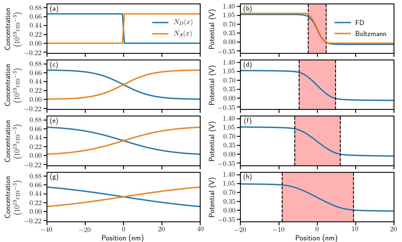
where , is the permitivity of the semiconductor prior to doping, and are the relative and vacuum permitivities respectively, and is the charge distribution. For sufficiently low doping, Eq. (2) can be solved assuming Boltzmann statistics, within the so-called full depletion approximation, where one obtains an analytical solution for the width of the depletion region [46]. However, estimations for acceptor () and donor () impurity concentrations from uniformly doped p and n-type SiNWs grown under similar conditions, are and , respectively, which are degenerate doping levels. And, our measured , eV, compares with the Si bandgap ( eV). Therefore, we also solved Eq. (2) numerically using Fermi-Dirac statistics. For the aforementioned and doping concentrations, and assuming an abrupt doping profile, we obtained a built-in potential of 1.173 V and a depletion region width of 4.7 nm. Details of this calculation can be found in the Supplemental Information.
Our measured depletion regions were larger than the prediction for abrupt junctions. Thus, it is interesting to model our junctions with a graded doping profile. Figure 6 compares the doping concentration profiles and depletion region widths calculated using both Boltzmann and Fermi-Dirac statistics, assuming maximum donor and acceptor impurity concentrations of cm-3 (i.e. the average of the experimental values of and ) and hyperbolic tangents for the graded doping transition (see Supplemental Information). Fits for these profiles were carried out using the same approach that was applied to the experimental data for meaningful comparison.
Figure 6 plots the doping profiles and the respective electric potential , as a function of the doping transition width (), assuming , 10, 20 and 60 nm, giving rise to depletion widths of , , and nm, respectively. The calculated depletion region width versus the doping transition width is plotted in Figure 7. A graded transition increases the width of the depletion region, as expected, and the values obtained are comparable to the measurements via EH.

All measured depletion regions were less than 20 nm with the exception of the n/p sequence of Growth 2, which showed a long depletion region ( nm) and highly defective junction. Existence of these junctions, including an irregular one corresponding to this growth and sequence, was confirmed via EBIC measurements (see Supplemental Information). In our experiments (Growth 2), we slowed down the growth rate nearby the junction to avoid the reservoir effect by allowing P or B to evaporate from the liquid catalyst. A high-angle annular dark-field (HAADF) STEM image as well as EDS maps and profiles of the defective n/p junction of Growth 2 are shown in Figure 8. Accumulation of Au is confirmed by the high-contrast regions in the HAADF image and by the EDS map of Au in Figure 8(b). Figure 8(c) and (d) show line profiles comparing the Si and Au EDS signals along the green and fuchsia boxes in Figure 8(b). A simple median filter was applied to the EDS data as a method of noise reduction [47].

Au deposited at the junction location (Growth 2, n/p sequence) according to Figure 8; however, SiNW growth was not hampered, as NWs reached their intended lengths ( m). Higher phase shifts (darker red coloration in Figure 4(f)) in the phase image as well as the profile peak (Figures 4(f) and (h)) are also a signature of Au accumulation at the junction. A calculation of the amount of Au in the direction of the beam for this profile yielded a maximum thickness of 9 nm (see Supplemental Information). Au is known to act as a surface passivator stabilizing epitaxial growth of <111> SiNWs [24, 44, 48, 49], and whenever this passivation is inhibited, SiNWs kink towards the more thermodynamically stable <112> direction. Au decoration is also known to happen randomly in highly-doped NW segments, dependent on pressure, growth rate, changes in the Au catalyst liquid volume and surface chemistry. Pressure and growth values exceeding 100 mTorr and 150 nm/min, respectively, are necessary to minimize this effect [44, 49].
Accumulation of Au at the junction interface is correlated with changes in the partial pressure of the precursors as described in Figure 1. If the change in SiH4 partial pressure alone was the cause, one would expect large Au deposits in the opposite growth sequence (p/n) as well, since the SiH4 partial pressure changes by the same magnitude. However, that was not the case. SiNWs resulting from Growth 2 in the p/n sequence showed negligible accumulation of Au. The most likely explanation is that the order in which one switches the gas precursors (PH3/B2H6) influences the Au segregation. The EDS map and profile in Figure 8(b) and (d), respectively, for growth in the n/p sequence show a nm transition of the P (n-type) dopant at the p-n interface. Relatively short doping transitions are expected since we followed growth conditions established in previous studies that lead to sharp P transitions[17]. The B dopant profile was not detected via EDS or electron energy loss spectroscopy due to a peak overlap produced by the Au and B signals. Figure 8(d) also shows a linear increase in the Si signal up to the junction region, where the Au has accumulated, while it remains constant in the n-type segment of the NW. This increase is likely due to changes in the AuSi catalyst contact angle during growth.
We did not observe charging induced by the electron beam in these NWs, therefore we can assume that the MIP values extracted from the calculated voltage profiles should occur at the midpoint of the voltage difference. The average values for both growths is V. Reported MIP values for Si are , V, and V experimentally determined through EH [50, 40]. Notice that our average MIP value is within the error of two of the previously reported values.
We obtained Vbi values that are comparable to the Si bandgap at RT in the p/n growth sequence for both types of growth. This was unexpected, since it has also been observed that measured Vbi values via EH can be up to 55% lower than expected [51]. Although these differences are known to increase for materials with larger bandgaps [28] and lower doping levels [52]. Interaction of the electron beam with the semiconducting NW generates currents due to SE emission and electron-hole pair generation, which can forward bias NWs decreasing the expected [53]. We attribute this apparent beam insensitivity to high dopant levels that decrease the NW carrier mobility and diffusion lengths, decreasing any beam induced charge accumulation. The long NW lengths created multiple contact points to the carbon support grid, aiding the neutralization of any shunt resistance developed while recording the data. However, we consistently obtained 0.2 - 0.3 V lower values for SiNWs in the n/p growth sequence. This could be attributed to residual PH3 in the reactor that causes compensation doping in the p-type segment. These values could be low enough to be out of the EDS detection limit and thus possibly at the noise level in Figure 8.
The characteristic NDR observed in tunnel junction I-V measurements was hidden likely due to excess currents originating from trap-assisted (TA) tunneling through mid-bandgap trap states[54]. Note that the indirect bandgap of Si tends to favor TA tunneling because of the momentum mismatch for direct band-to-band (BB) tunneling. The TA tunneling rate is also substantially higher than BB tunneling except in very high electric fields [55]. Unlike band-to-band tunneling, trap-assisted tunneling is temperature-dependent and cooling down the device can increase the peak-to-valley current ratio and reveal NDR behavior [18]. The change in slope observed near V (Figure 5) in low temperature I-V curves resemble those previously seen in Au-doped planar Si tunnel junctions [54], suggesting that our tunnel junctions are conducting via the same mechanism. Since we have little control over the gold defect density in the NWs during our VLS growth process, the resistance of the NWs can vary noticeably between NWs from the same synthesis. However, NDR, a hallmark of tunneling behavior, was observed for one NW (Figure S8) likely because it had an unusually low Au defect density at the junction, but also because it was grown in the Growth 2 p/n sequence, which exhibited the shortest depletion width of all conditions studied. At the opposite extreme, when Au concentration is very high, such as those observed via EDS in Growth 2 n/p sequence, the junctions are electrically shorted, and their average resistivity ( m) is consistent with reported values for heavily-doped n- and p-type bulk Si [56]. The other growth sequences exhibit higher resistivity values (Table S1) as expected, dominated by the junction resistance.
Conclusions
We have used electron holography (EH) to characterize depletion regions of heavily-doped, VLS-grown SiNWs. We compared the effects of growth conditions and sequence order: p/n and n/p with the aim of optimizing tunneling junctions. Keeping the partial pressure of the precursors constant (Growth 1) yielded narrow depletion regions of nm and nm for p/n and n/p, respectively. Slowing the growth rate at the junction region (Growth 2) increased the junction abruptness, decreasing the depletion width to nm in the case of the p to n switching. However, slower switching also created more instabilities in the Au catalyst leading to more kinking in the majority of the NWs. Slower growth in the n to p sequence substantially increased the degree of segregation of Au particles from the catalyst seed. Measured Vbi values were higher and comparable to the Si bandgap for the p/n sequence ( and V) than for the n/p sequence ( and V) in both types of growth, potentially due to PH3 doping compensation in the p-type segment of the n/p sequence.
Overall, the results have confirmed the existence of electrically abrupt, degenerately-doped axial SiNW junctions that exhibit tunnel-junction behavior in both sequences (p/n and n/p). The width of the depletion regions could be as short as nm using optimal growth rates and sequences. This is the first essential step in the creation of more complex solar energy devices and possibly other technologies that require tunnel junctions, such as tunneling field-effect transistors and multijunction solar cells.
Methods
Nanowire synthesis
SiNWs were synthesized in a home-built chemical vapor deposition (CVD) system [17, 19, 21, 44]. Au catalysts of nm diameter were immobilized on SiO2 wafers. This thermally-grown SiO2 (300 nm) in the wafer made the nucleation and growth happen preferably in the <112> growth direction. Silane (SiH4) was the Si source, diborane (B2H6, 1000 ppm in H2) and phosphine (PH3, 1000 ppm in H2) served as p and n-type dopant precursors, respectively. Hydrochloric acid (HCl ) was used for chlorination and H2 as the carrier gas. Growth was carried out at 510∘C, total pressure of 20 Torr and a HCl:SiH4 ratio of 2:1 for both types of growth.
Growth 1
For the p/n sequence, we first grew 10 - 15 m highly-doped p-type at a growth rate of 320 nm/min and abruptly switched the dopant precursor to n-type with a growth rate of 260 nm/min, until the end of the NW growth (1.4 m). For the n/p sequence we first grew 5 m p-type followed by 12 m of highly n-doped segment at a growth rate of 280 nm/min until abruptly switching to p-type with grow rate of 280 nm/min for five minutes (1.6 m) until the end of the growth.
Growth 2
For the p/n sequence, we first grew 10 - 15 m of highly p-doped segment at a growth rate of 320 nm/min, then, we dropped the growth rate to 32 nm/min for two minutes until abruptly stopping the flow of the diborane precursor. At the same time the phosphane precursor was turned on with a growth rate of 28 nm/min. Finally, after 2 mins ( nm) the growth rate was increased back to 280 nm/min. For the opposite sequence (n/p), nucleation started with 3 m of undoped Si, followed by 12 m of n-doped Si at a growth rate of 280 nm/min. Then the growth rate was decreased to 28 nm/min for two minutes until abruptly stopped. The p-type precursor was started immediately after at a growth rate of 32 nm/min for two minutes. Finally, the growth rate was increased back to 320 nm/min. The Si precursor to dopant precursor ratios (SiH4:PH3, SiH4:B2H6) remained constant in both cases.
TEM sample preparation and imaging
TEM sample preparation was carried out by mechanical abrasion of NWs directly onto lacey carbon support grids, to avoid artifacts or NW modification created by solvents. EH data was collected using electrons generated by a field-emission gun, operated at an acceleration voltage of 200 kV in a scanning transmission electron microscope (STEM) with point to point resolution of 0.23 nm (FEI Tecnai G2) using the objective lens for TEM imaging and a Lorentz lens for EH, which gives a wider field of view. The exposure time was 1.5 s and the biprism voltage 140 V. The reference hologram was obtained 800 nm from the NW axis for a magnification of 33 kX, following the optimum position for an empty hologram procedure [57, 58]. Higher magnification images were acquired on a Hitachi HF-3300 TEM, HF-3300V scanning transmission electron holography microscope (STEHM) cold-field-emmision electron source, operated at an acceleration voltage of 300 kV which can achieve both a STEM electron probe size and TEM spatial resolution approaching 45 pm. Finally, STEM and energy dispersive x-ray spectroscopy maps were obtained using a STEM (FEI Osiris) operated at 200 keV with a STEM resolution of 0.16 nm.
Current-voltage measurements
SiNWs were mechanically transferred from the growth substrate onto Si/SiO2/SiN4 wafers. A photo-resist stack (MMA EL9 and PMMA A2, Microchem) was spun on top of the NWs and contacts to single NWs were patterned via electron beam lithography (Nanometer Pattern Generation System). The native oxide was etched from the patterned area using buffered hydrofluoric acid (Transene) and metal electrodes (3 nm Ti, 300 nm Pd) were deposited with electron beam evaporation (KJ Lesker PVD 75). Each NW was contacted by four electrodes to ensure that the contacts were ohmic. Current-voltage measurements at ambient conditions were taken with a Keithley 2636A SourceMeter connected to a pair of micropositioners (Signatone, S-725) and probe tips (SE-TL, tungsten). For low temperature measurements, the NWs were tested in a cryogenic probe station (Lakeshore PS-100) under vacuum and cooled with liquid nitrogen.
References
- [1] R. Singh. Why silicon is and will remain the dominant photovoltaic material. Journal of Nanophotonics, 3(1):032503–032503, July 2009.
- [2] Joern Huenteler, Tobias Schmidt, Jan Ossenbrink, and Volker Hoffmann. Technology life-cycles in the energy sector - technological characteristics and the role of deployment for innovation. Technological Forecasting and Social Change, 104:102–121, 2016.
- [3] Y. M. Yang, A. Yu, B. Hsu, W. C. Hsu, A. Yang, and C. W. Lan. Development of high-performance multicrystalline silicon for photovoltaic industry: High-performance mc-si for photovoltaic industry. Progress in Photovoltaics: Research and Applications, 23(3):340–351, 2015.
- [4] Nisreen Shehada, John C Cancilla, Jose S Torrecilla, Enrique S Pariente, Gerald Brönstrup, Silke Christiansen, Douglas W Johnson, Marcis Leja, Michael P A Davies, Ori Liran, Nir Peled, and Hossam Haick. Silicon nanowire sensors enable diagnosis of patients via exhaled breath. ACS Nano, 10(7):7047–7057, 2016.
- [5] Weiyi Zhang, Ming Hu, Xing Liu, Yulong Wei, Na Li, and Yuxiang Qin. Synthesis of the cactus-like silicon nanowires/tungsten oxide nanowires composite for room-temperature no2 gas sensor. Journal of Alloys and Compounds, 679:391–399, 2016.
- [6] Fouad Demami, Liang Ni, Regis Rogel, Anne-Claire Salaün, and Laurent Pichon. Silicon nanowires based resistors as gas sensors. Sensors and Actuators B: Chemical, 170(C):158–162, 2011.
- [7] Xiaolei Wang, Ge Li, Min Ho Seo, Gregory Lui, Fathy M Hassan, Kun Feng, Xingcheng Xiao, and Zhongwei Chen. Carbon-coated silicon nanowires on carbon fabric as self-supported electrodes for flexible lithium-ion batteries. ACS Applied Materials ’I&’ Interfaces, 9(11):9551–9558, 2017.
- [8] David Aradilla, Fang Gao, Georgia Lewes-Malandrakis, Wolfgang Müller-Sebert, Pascal Gentile, Stéphanie Pouget, Christoph E. Nebel, and Gérard Bidan. Powering electrodes for high performance aqueous micro-supercapacitors: Diamond-coated silicon nanowires operating at a wide cell voltage of 3 v. Electrochimica Acta, 242:173–179, 2017.
- [9] Ray LaPierre and Mahendra Sunkara. Nanowires for energy. Nanotechnology, 23(19):190201–190201, apr 2012.
- [10] L. Esaki and Y. Miyahara. A new device using the tunneling process in narrow p-n junctions. Solid State Electronics, 1:13, March 1960.
- [11] M. Heurlin, P. Wickert, S. Fält, M. T. Borgström, K. Deppert, L. Samuelson, and M. H. Magnusson. Axial InP nanowire tandem junction grown on a silicon substrate. Nano Letters, 11:2028–2031, May 2011.
- [12] Jesper Wallentin, Johan M. Persson, Jakob B. Wagner, Lars Samuelson, Knut Deppert, and Magnus T. Borgström. High-performance single nanowire tunnel diodes. Nano Letters, 10(3):974–979, 2010.
- [13] Xulu Zeng, Gaute Otnes, Magnus Heurlin, Renato T. Mourão, and Magnus T. Borgström. InP/GaInP nanowire tunnel diodes. Nano Research, 11(5):2523–2531, May 2018.
- [14] Martin Ek, B. Mattias Borg, Anil W. Dey, Bahram Ganjipour, Claes Thelander, Lars-Erik Wernersson, and Kimberly A. Dick. Formation of the axial heterojunction in gasb/inas(sb) nanowires with high crystal quality. Crystal Growth ’I&’ Design, 11(10):4588–4593, 2011.
- [15] Bahram Ganjipour, Anil W. Dey, B. Mattias Borg, Martin Ek, Mats-Erik Pistol, Kimberly A. Dick, Lars-Erik Wernersson, and Claes Thelander. High current density esaki tunnel diodes based on GaSb-InAsSb heterostructure nanowires. Nano Letters, 11(10):4222–4226, 2011.
- [16] B. Mattias Borg, Martin Ek, Bahram Ganjipour, Anil W. Dey, Kimberly A. Dick, Lars-Erik Wernersson, and Claes Thelander. Influence of doping on the electronic transport in gasb/inas(sb) nanowire tunnel devices. Applied Physics Letters, 101(4):043508, 2012.
- [17] Joseph D Christesen, Christopher W Pinion, Xing Zhang, James R Mcbride, and James F Cahoon. Encoding abrupt and uniform dopant profiles in vapor-liquid-solid nanowires by suppressing the reservoir effect of the liquid catalyst. ACS Nano, 8(11):11790–11798, 2014.
- [18] Heinz Schmid, Cedric Bessire, Mikael T Björk, Andreas Schenk, and Heike Riel. Silicon nanowire esaki diodes. Nano Letters, 12(2):699–703, 2012.
- [19] David J Hill, Taylor S Teitsworth, Seokhyoung Kim, Joseph D Christesen, and James F Cahoon. Encoding highly nonequilibrium boron concentrations and abrupt morphology in p-type/n-type silicon nanowire superlattices. ACS Applied Materials ’I&’ Interfaces, 9(42):37105–37111, 2017.
- [20] Thomas J Kempa, Bozhi Tian, Dong Rip Kim, Jinsong Hu, Xiaolin Zheng, and Charles M Lieber. Single and tandem axial p-i-n nanowire photovoltaic devices. Nano Letters, 8(10):3456–3460, 2008.
- [21] Christopher W. Pinion, Joseph D. Christesen, and James F. Cahoon. Understanding the vaporliquidsolid mechanism of si nanowire growth and doping to synthetically encode precise nanoscale morphology. Journal of Materials Chemistry C, 4(18):3890–3897, 2016.
- [22] Chito Kendrick, Meng-Wei Kuo, Jie Li, Haoting Shen, Theresa S. Mayer, and Joan M. Redwing. Uniform p-type doping of silicon nanowires synthesized via vapor-liquid-solid growth with silicon tetrachloride. Journal of Applied Physics, 122(23):235101, 2017.
- [23] Joseph D Christesen, Christopher W Pinion, David J Hill, Seokhyoung Kim, and James F Cahoon. Chemically engraving semiconductor nanowires: Using three-dimensional nanoscale morphology to encode functionality from the bottom up. The Journal of Physical Chemistry Letters, 7(4):685–692, 2016.
- [24] Ling Pan, Kok-Keong Lew, Joan M. Redwing, and Elizabeth C. Dickey. Effect of diborane on the microstructure of boron-doped silicon nanowires. Journal of Crystal Growth, 277(1-4):428–436, 2005.
- [25] Joseph D Christesen, Christopher W Pinion, Erik M Grumstrup, John M Papanikolas, and James F Cahoon. Synthetically encoding 10 nm morphology in silicon nanowires. Nano Letters, 13(12):6281–6286, 2013.
- [26] Cordelia P. Sealy, Peter R. Wilshaw, and Martin R. Castell. Mechanism for secondary electron dopant contrast in the SEM. Journal of Electron Microscopy, 49(2):311–321, 01 2000.
- [27] M. Molotskii, Z. Barkay, J. Marczewski, P. Grabiec, I Volotsenko, M Molotskii, Z Barkay, J Marczewski, P Grabiec, B Jaroszewicz, G Meshulam, E Grunbaum, and Y Rosenwaks. Secondary electron doping contrast: Theory based on scanning electron microscope and kelvin probe force microscopy measurements. Journal of Applied Physics., 107(1):014510, 2010.
- [28] Sadegh Yazdi, Alexander Berg, Magnus T Borgström, Takeshi Kasama, Marco Beleggia, Lars Samuelson, and Jakob B Wagner. Doping gap core-shell nanowire pn-junctions: A study by off-axis electron holography. Small (Weinheim an der Bergstrasse, Germany), 11(22):2687–2695, 2015.
- [29] Ali Darbandi, James C Mcneil, Azadeh Akhtari-Zavareh, Simon P Watkins, and Karen L Kavanagh. Direct measurement of the electrical abruptness of a nanowire p-n junction. Nano Letters, 16(7):3982–3988, 2016.
- [30] M. I. den Hertog, H. Schmid, D. Cooper, J.-L. Rouviere, M.T. Björk, H. Riel, P. Rivallin, S. Karg, and W. Riess. Mapping active dopants in single silicon nanowires using off-axis electron holography. Nano Letters, 9:3837–3843, November 2009.
- [31] Z. Gan, D. E. Perea, J. Yoo, S. Tom Picraux, D. J. Smith, and M. R. McCartney. Mapping electrostatic profiles across axial p-n junctions in Si nanowires using off-axis electron holography. Applied Physics Letters, 103(15):153108, October 2013.
- [32] Myung-Geun Han, Joseph A. Garlow, Matthew S.J. Marshall, Amanda L. Tiano, Stanislaus S. Wong, Sang-Wook Cheong, Frederick J. Walker, Charles H. Ahn, and Yimei Zhu. Electron-beam-induced-current and active secondary-electron voltage-contrast with aberration-corrected electron probes. Ultramicroscopy, 176:80–85, 2017.
- [33] S. P. Watkins, A Darbandi, and S P Watkins. Measurement of minority carrier diffusion lengths in gaas nanowires by a nanoprobe technique. Journal of Applied Physics., 120(1):014301, 2016.
- [34] E Koren, J K Hyun, U Givan, E R Hemesath, L J Lauhon, and Y Rosenwaks. Obtaining uniform dopant distributions in vls-grown si nanowires. Nano Letters, 11(1):183–187, 2011.
- [35] S Vinaji, A Lochthofen, W Mertin, I Regolin, C Gutsche, W Prost, F J Tegude, and G Bacher. Material and doping transitions in single gaas-based nanowires probed by kelvin probe force microscopy. Nanotechnology, 20(38):385702, 2009.
- [36] V. Brouzet, B. Salem, P. Periwal, G. Rosaz, T. Baron, F. Bassani, P. Gentile, and G. Ghibaudo. Fabrication and characterization of silicon nanowire p-i-n mos gated diode for use as p-type tunnel fet. Applied Physics A, 121(3):1285–1290, 2015.
- [37] Aaron L Vallett, Sharis Minassian, Phil Kaszuba, Suman Datta, Joan M Redwing, and Theresa S Mayer. Fabrication and characterization of axially doped silicon nanowire tunnel field-effect transistors. Nano Letters, 10(12):4813–4818, 2010.
- [38] Earl T Ritchie, David J Hill, Tucker M Mastin, Panfilo C Deguzman, James F Cahoon, and Joanna M Atkin. Mapping free-carriers in multijunction silicon nanowires using infrared near-field optical microscopy. Nano Letters, 17(11):6591, 2017.
- [39] Zhiyuan Sun, David N Seidman, and Lincoln J Lauhon. Nanowire kinking modulates doping profiles by reshaping the liquid-solid growth interface. Nano Letters, 17(7):4518–4525, 2017.
- [40] L Wu, M.A Schofield, Y Zhu, and J Tafto. A unique determination of boundary condition in quantitative electron diffraction: Application to accurate measurements of mean inner potentials. Ultramicroscopy, 98(2):135–143, 2004.
- [41] D. Cooper, R. Truche, A. C. Twitchett-Harrison, R. E. Dunin-Borkowski, and P. A. Midgley. Quantitative off-axis electron holography of GaAs p-n junctions prepared by focused ion beam milling. Journal of Microscopy, 233(1):102–113.
- [42] S Yazdi, T Kasama, R Ciechonski, O Kryliouk, and J B Wagner. The measurement of electrostatic potentials in core/shell gan nanowires using off-axis electron holography. Journal of Physics: Conference Series, 471(1):012041, 2013.
- [43] K. He, J.-H. Cho, Y. Jung, S. T. Picraux, and J. Cumings. Silicon nanowires: Electron holography studies of doped p-n junctions and biased Schottky barriers. Nanotechnology, 24(11):115703, March 2013.
- [44] Seokhyoung Kim, David J. Hill, Christopher W. Pinion, Joseph D. Christesen, James R. McBride, and James F. Cahoon. Designing morphology in epitaxial silicon nanowires: The role of gold, surface chemistry, and phosphorus doping. ACS Nano, 11(5):4453–4462, 2017.
- [45] N. W. Ashcroft and N. D. Mermin. Solid State Physics. Saunders College, Philadelphia, PA, 1976.
- [46] Ben G. Streetman and Sanjay Banerjee. Solid state electronic devives. Prentice-Hall series in solid state physical electronics, 5th ed. edition, 2000.
- [47] David C Stone. Application of median filtering to noisy data. Canadian Journal of Chemistry, 73(10):1573–1581, 1995.
- [48] Heinz Schmid, Mikael T Björk, Joachim Knoch, Siegfried Karg, Heike Riel, and Walter Riess. Doping limits of grown in situ doped silicon nanowires using phosphine. Nano Letters, 9(1):173–177, 2009.
- [49] Eric Dailey, Prashanth Madras, and Jeff Drucker. Au on vapor-liquid-solid grown si nanowires: Spreading of liquid ausi from the catalytic seed. Journal of Applied Physics, 108(6):064320, 2010.
- [50] P. Kruse, M. Schowalter, D. Lamoen, A. Rosenauer, and D. Gerthsen. Determination of the mean inner potential in III-V semiconductors, Si and Ge by density functional theory and electron holography. Ultramicroscopy, 106(2):105–113, 2006.
- [51] D. Wolf, A. Lubk, A. Lenk, S. Sturm, and H. Lichte. Tomographic investigation of fermi level pinning at focused ion beam milled semiconductor surfaces. Applied Physics Letters, 103(26):264104, 2013.
- [52] L. Houben and M. Luysberg. Illumination effects in holographic imaging of the electrostatic potential of defects and pn junctions in transmission electron microscopy. Physical Review. B, Condensed Matter and Materials Physics, 70(16):165313, 2004.
- [53] Cristina Cordoba, Xulu Zeng, Daniel Wolf, Magnus T Borgström, Enrique Barrigón, Axel Lubk, and Karen L Kavanagh. Three-dimensional imaging of beam-induced biasing of inp/gainp tunnel diodes. Nano Letters, 19(6):3490–3497, 2019.
- [54] C. T. Sah. Electronic processes and excess currents in gold-doped narrow silicon junctions. Physical Review, 123(5):1594–1612, 1961.
- [55] A. Schenk. Rigorous theory and simplified model of the band-to-band tunneling in silicon. Solid-State Electronics, 36(1):19 – 34, 1993.
- [56] G Masetti, M Severi, and S Solmi. Modeling of carrier mobility against carrier concentration in arsenic-, phosphorus-, and boron-doped silicon. IEEE Transactions on Electron Devices, 30(7):764–769, 1983.
- [57] Daniel Wolf, Axel Lubk, Hannes Lichte, and Heiner Friedrich. Towards automated electron holographic tomography for 3D mapping of electrostatic potentials. Ultramicroscopy, 110(5):390–399, 2010.
- [58] Leigang Kou and Jianwen Chen. Eliminating the influence of the perturbed reference wave in electron holography. Journal of Modern Optics, 42(6):1171–1178, 1995.