A N-Path Receiver With Harmonic Response Suppression
Abstract
A downconversion receiver employing a switch-based N-path filter with reduced harmonic response around the third- and fifth- LO harmonics is presented. The N-path filter is placed in a frequency-translation feedback loop that is effective at the and the LO harmonics to mitigate harmonic downconversion. A pulse-width-modulated LO (PWM-LO) clocking scheme is used in the feedback upconverter to reduce the noise injected around the LO harmonic at the input of N-path downconverter. The compression resulting from blockers around the and the LO harmonics is also suppressed as a result of reduced harmonic response. Compensation of peak frequency shift of the N-path response due to parasitic input capacitance is also described.
Index Terms:
N-path filter, Harmonic ResponseI Introduction
A switched-capacitor N-path circuit[1] can be employed for filtering an RF signal as well as a passive downconverter. Switch-based implementations of such filters have been demonstrated in recent literature, e.g., [2]. N-path filters can provide a high effective quality factor, a high dynamic range and a tunable response, in addition to being scalable with process technology [3].
A known limitation of a switch-based N-path filter is that in addition to downconverting signals around the desired center frequency, the circuit also downconverts signals located around harmonics of the center frequency. An approach to reduce the harmonic response employing a PWM representation of a sinusoidal clock was shown in [4]. An N-path filter with a fundamental response at that employs rectangular clocks requires a primary clock frequency of . With PWM clocks, the primary clock frequency is , where the degree of harmonic suppression improves with increasing . For and , the approach effectively removes harmonic response up to nearly as shown in [4]. A challenge of the approach is the requirement for high PWM clock frequency, which can limit the achievable harmonic suppression due to narrow pulse-widths.
Mixer-first receivers that provide cancellation of LO harmonic responses at the receiver output have been demonstrated in prior literature [5, 6, 7]. The goal of this work is to provide harmonic response suppression at the input of the N-path filter, similar to [4], without the requirement for high clock frequency. A frequency-translation feedback loop is used in the proposed approach. The use of a frequency-translation loop for input matching and enhancing out-of-band blocker performance near the fundamental LO frequency of a receiver was shown in [8]. Feedback-based interference-rejection in a broadband channelizer using reconfigurable harmonic rejection mixers in the feedforward and feedback paths for suppression of harmonic LO levels was described in [9].

In this work, an eight-phase, N-path receiver that suppresses the response around the and the harmonics of the fundamental LO frequency, , at the RF input is proposed. The design employs capacitive baseband loads. The N-path filter by itself provides a bandpass response at the fundamental LO frequency and all odd harmonics of the LO, with bandwidth determined by the baseband capacitors and the source resistance [10].

In order to suppress the input response from the harmonics of the LO, the baseband signal components downconverted by the and the harmonics of the LO signal at the output of the N-path filter, are upconverted in a harmonic-selective feedback path to the input. The feedback path operates only around the and the harmonics. This is ensured by using a baseband harmonic selective combiner, that selects only these signal components, and rejects the signal downconverted by the fundamental . In addition, the feedback path upconverter employs a pulse-width-modulated LO (PWM-LO) with an ideally zero component around and primary harmonics at and [11][12] as described below.
Suppressing the harmonic response at the RF input also ensures similar suppression at the baseband output. Combined with another baseband harmonic rejection stage which selects baseband signals downconverted from the fundamental, the architecture is shown to provide harmonic rejection of nearly a two-stage harmonic rejection downconverter [13][14]. The filter response at is not mitigated by the architecture, for , however it assumed that the inherent attenuation provided by the N-path filter at baseband is adequate.
The architecture is described in Section II. An approach for avoiding the frequency-shift in the response caused by a parasitic input capacitance [15] is also described. Section III describes simulation-based results and the conclusion follows in Section IV.
II Overview of the Architecture
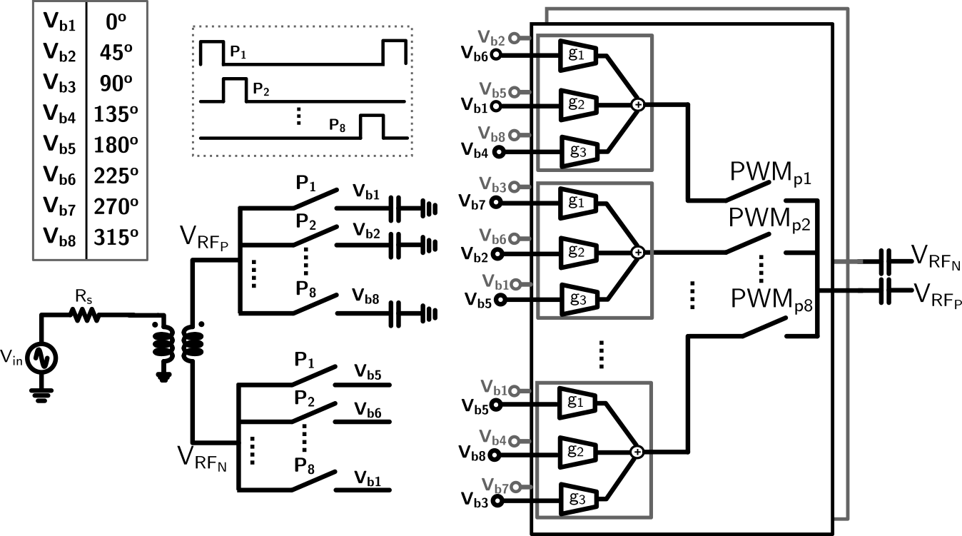
The receiver architecture is shown in Fig. 1. The architecture consists of a main-loop, which provides the N-path filtering at the input, and the baseband signals, and two harmonic rejection combiners, one within the loop (HR2), and one outside the loop (HR1). HR1 selects signals downconverted around , while HR2 selects signals dowconverted from around and The design of these is described below.
II-A The Main Loop
The main-loop in the proposed architecture employs an N-path filter, a baseband harmonic rejection stage (HR2) to reject the fundamental and amplify the and the harmonics, and a passive-mixer based upconverter as shown in Fig. 1. The N-path filter consists of NMOS switches with capacitive loads at the output, while HR2 is a transconductance-based harmonic-selection stage, which employs -ratios to suppress or enhance specific harmonics.
HR2 suppresses the baseband signal that is downconverted from by the N-path filter, but since it uses active devices, baseband noise, including flicker noise, appears at its output. It is critical to ensure that this noise does not get translated to around at the input of the N-path filter, since this can severely degrade the noise figure of the desired signal at this frequency. To ensure this, the upconverter employs a pulse-width-modulated (PWM-LO) that has an attenuated fundamental LO component, but large and nominally equal LO components at and . This clock upconverts the baseband signal components downconverted by the N-path filter by these harmonics, while suppressing the upconversion of baseband noise at the output of HR2 to . Noise components around and at the output of HR2, which can also be translated to by the PWM-LO are suppressed by capacitance at the output of HR2. The negative feedback provided by the loop ensures that a low input impedance is achieved around the and the harmonics, thereby suppressing the signal at this node. The differential nature of the implementation inherently rejects even harmonics.
While a PWM-LO approach is employed here, it is also possible to upconvert the baseband signal components from the N-path filter output to RF using a passive mixer, and then employ harmonic selection in HR2 to attenuate the upconverted component around Doing so avoids the baseband flicker noise of HR2 from degrading the noise figure at . However HR2 noise at can directly appear at the input to the N-path filter. To mitigate this, an HPF is required in the signal path with a stop-band around and a pass-band around and (Fig. 2(b)). This filter needs to be passive as the use of active devices would contribute additional device noise at in the filter itself. While an approach such as [16] can be employed, design of this filter is challenging since the loop presents a low-impedance at the filter output at and , and a larger impedance at , which works against achieving a high-pass response from the filter.
A more subtle issue arises if a passive mixer is directly connected between the N-path baseband capacitors, and the inputs of the HR2 devices. The passive mixer cyclically connects the baseband outputs of the N-path filter to any one input of the HR2 devices. This leads to charge sharing between the baseband capacitors of the N-path filter which should be ideally isolated from each other. This in turn leads to a frequency shift of the input response of the N-path. This effect is similar to the frequency shift caused by a parasitic capacitor at the input of the N-path filter itself, as described in [15].
For the above reasons, the approach of Fig. 2(a) is employed in the proposed design.
II-A1 N-Path Filter Design
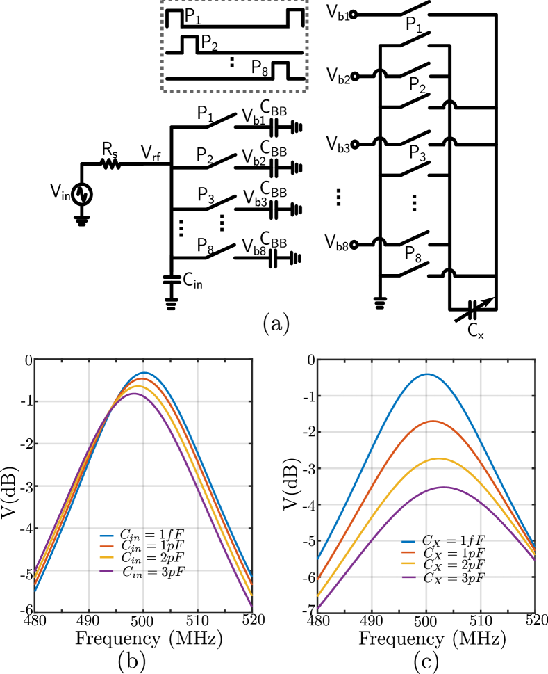
The main-loop in the proposed architecture employs an N-path filter with eight-phase rectangular, non-overlapping clocks. The switches are loaded by capacitors and the baseband outputs are observed across these capacitors (Fig. 3(a)).
It has been observed that the fundamental response at the node in Fig. 3(a) shifts left due to the parasitic capacitance at the node [15] as shown in Fig. 3(b), for different values of This frequency-shift appears because correlates the charge held on baseband capacitors across phases To compensate for the left shift of the peak due to , the circuit shown in Fig. 3(a) is proposed. A toggling capacitor is applied to the outputs . is connected across , with alternating polarity as the clock progresses from to . The capacitor resets the residual charge held by at the start of each pulse phase, thus preventing frequency shift.111This correction is not fundamental to the functioning of the receiver loop itself, but is beneficial for centering the frequency response.
As shown in Fig. 3(c), as increases for = 0, the fundamental response at shifts to the right of . For a non-zero , the frequency response of the N-path can be centered accurately around , by choosing appropriate value of . The use of also provides loss at the input, which is used to achieve input matching instead of an input resistance.
A similar approach as the above, which is used to compensate the impact of can also be employed to compensate the impact of the parasitic capacitance at the output of the passive mixer in the approach of Fig. 2(b). However, a very large value of may be required in that case, which leads to excessive attenuation at the input of the N-path filter.
II-A2 Baseband Harmonic Rejection Combiner (HR2)
The outputs of the N-path downconverter at baseband are combined using the harmonic rejection combiner (HR2), which is designed to reject the fundamental while amplifying the and the harmonics. The harmonic rejection is performed before upconverting the 8 baseband signals, using baseband cells with ideal gain ratios of , implemented in practice using integer ratios of . The output of HR2 is fed to the upconverter, the output of which is fed back to the RF input of the N-path filter. Since the upconverted signal does not consist of a component around the LO fundamental, the feedback-loop is ineffective at this frequency, and has an ideal loop-gain of zero. On the other hand, the gain of HR2 at the and the harmonics ensures an open-loop gain given by the product of the downconversion and upconversion paths.
Figure 4 represents the circuit used for implementing the harmonic rejection mixer. The inputs to gain coefficients and are rotated by compared to the inputs of to suppress the fundamental harmonic.
II-A3 Noise Suppression Using PWM Upconverter
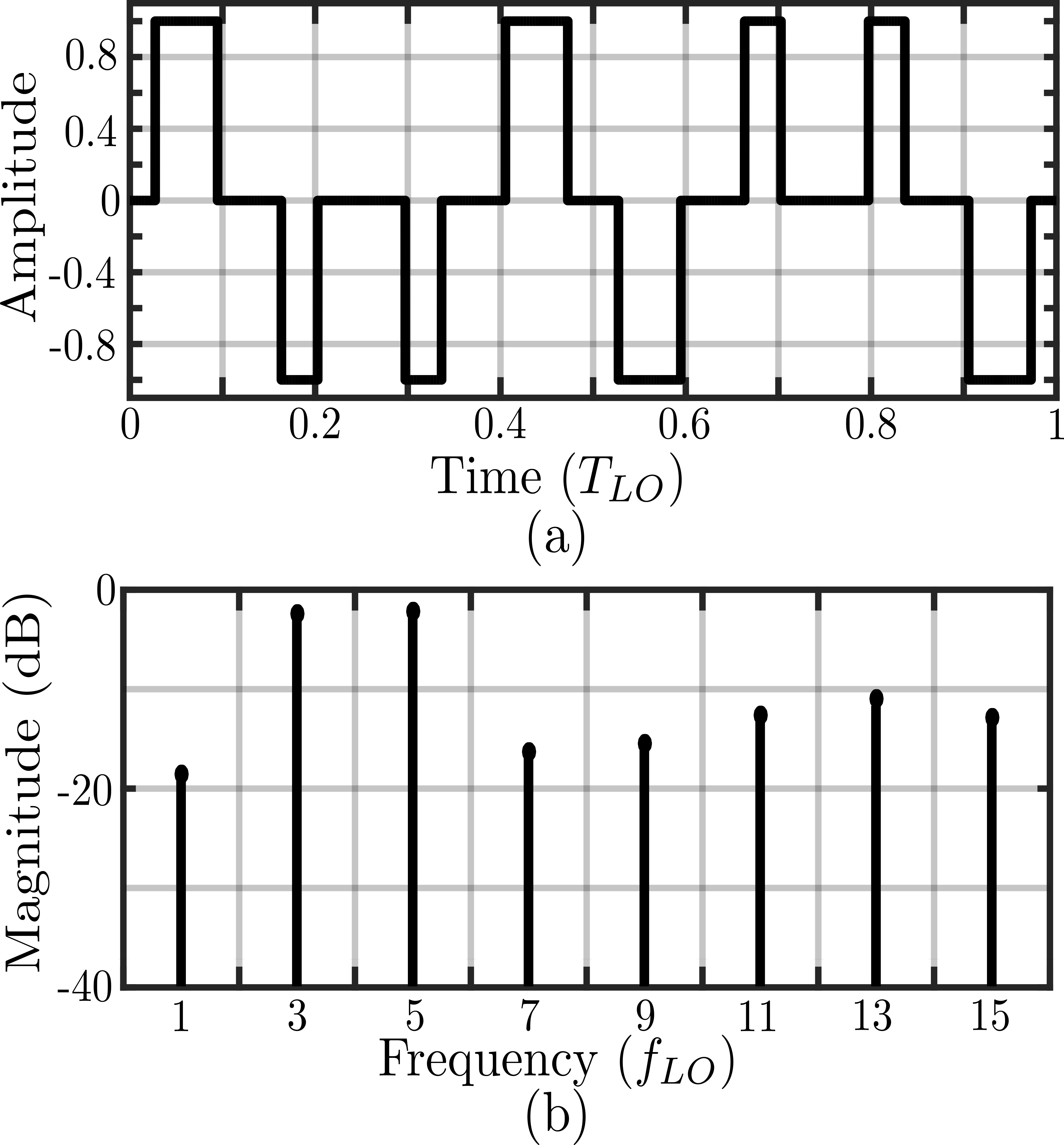
As noted above, while HR2 rejects the signal component at , it introduces baseband flicker noise at its output due to the use of active devices in the design. The response of the upconverter around is suppressed by using a PWM-LO clock.
The PWM-LO waveform in the time-domain and its frequency response is shown in Fig. 5. The PWM-LO is divided into two pulse sequences, corresponding to the positive and negative polarity of the time-domain waveform. The PWM upconverter consists of two switch banks driven by either the positive or negative pulse sequence. For example, in Fig. 4 represents all the positive pulses in the PWM waveform shown in Fig. 5(a). (Fig. 4) is synthesized by shifting by one period of the primary clock (). All the mixer outputs clocked by are combined and applied to the positive input of the N-path. Similarly, in Fig. 4 represents all the negative pulses in the PWM waveform shown in Fig. 5(a). is synthesized by shifting by one period of the primary clock ()). All the mixer outputs clocked by are combined and applied to the negative input of N-path.
An approach for generating high-frequency PWM clocks is described in [11]. The approach uses a voltage-controlled delay line (VCDL) within a delay locked loop (DLL), and can be employed here.
II-B Baseband Harmonic Rejection Combiner
A harmonic rejection combiner (HR1) is used to combine the 8-phase baseband signals and provide differential quadrature outputs , and ,. The baseband combiner uses a combiner [17], employing suitably scaled transconductance () cells (12:17:12 in this case). The outputs of the cells are applied to transimpedance amplifiers (TIAs), that convert the current outputs of these cells to voltages.
The feedback loop provides rejection of the harmonic responses around and at the RF input, and at the baseband outputs of the N-path downconverter. The use of HR1 provides effectively a second-stage of harmonic rejection.
III Simulation results
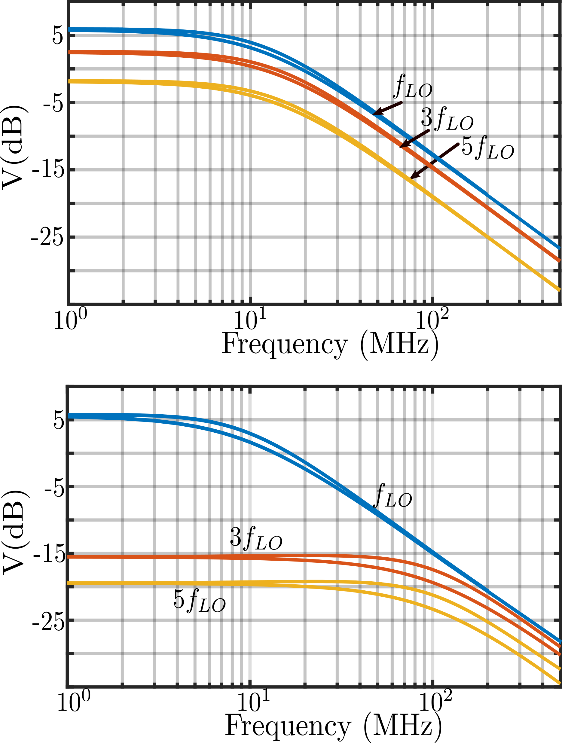
Simulations of the proposed architecture of Fig. 1 are shown below. The design is simulated and verified using a 65-nm commercial CMOS process, which includes the complete device model. The design employs an 8-phase clock with = 500 MHz. The harmonic responses at the baseband of an N-path filter by itself, and for the main-loop shown in Fig. 1 are shown in Fig. 6. The input frequency is swept from 300 MHz - 3 GHz and the frequency-translated output at baseband is observed. The baseband components downconverted from and can be seen to be reduced to nearly 20 and 25 dB relative to the component from , respectively, with the feedback loop, compared to approximately 3 dB and 6 dB respectively for the N-path filter by itself.
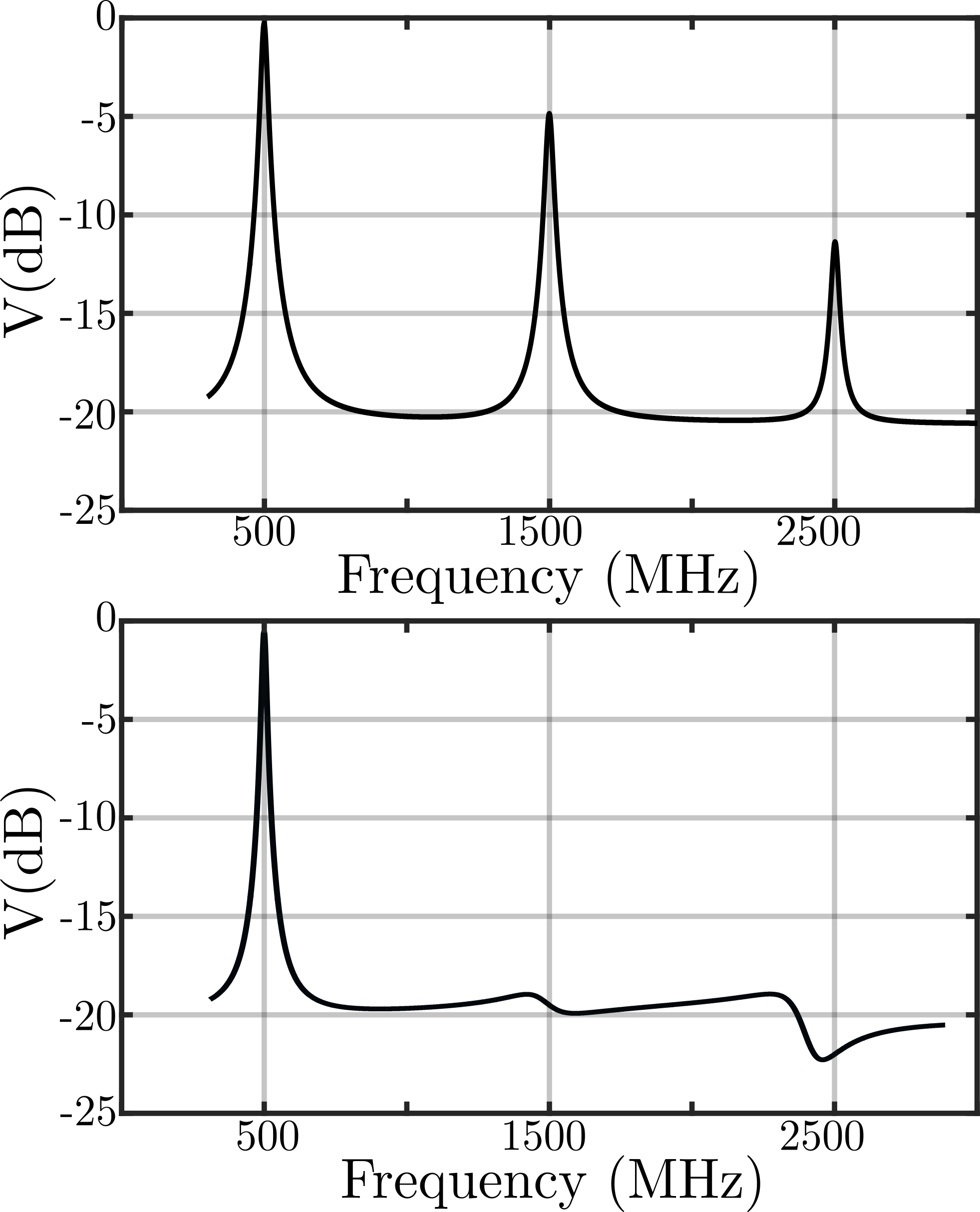
The RF response for the above two cases is compared in Fig. 7. The default N-path filter exhibits downconversion from all odd harmonics of , while the main-loop shows a response only at , and thus resembles an ideal BPF. The floor of the response is set by the switch resistance.
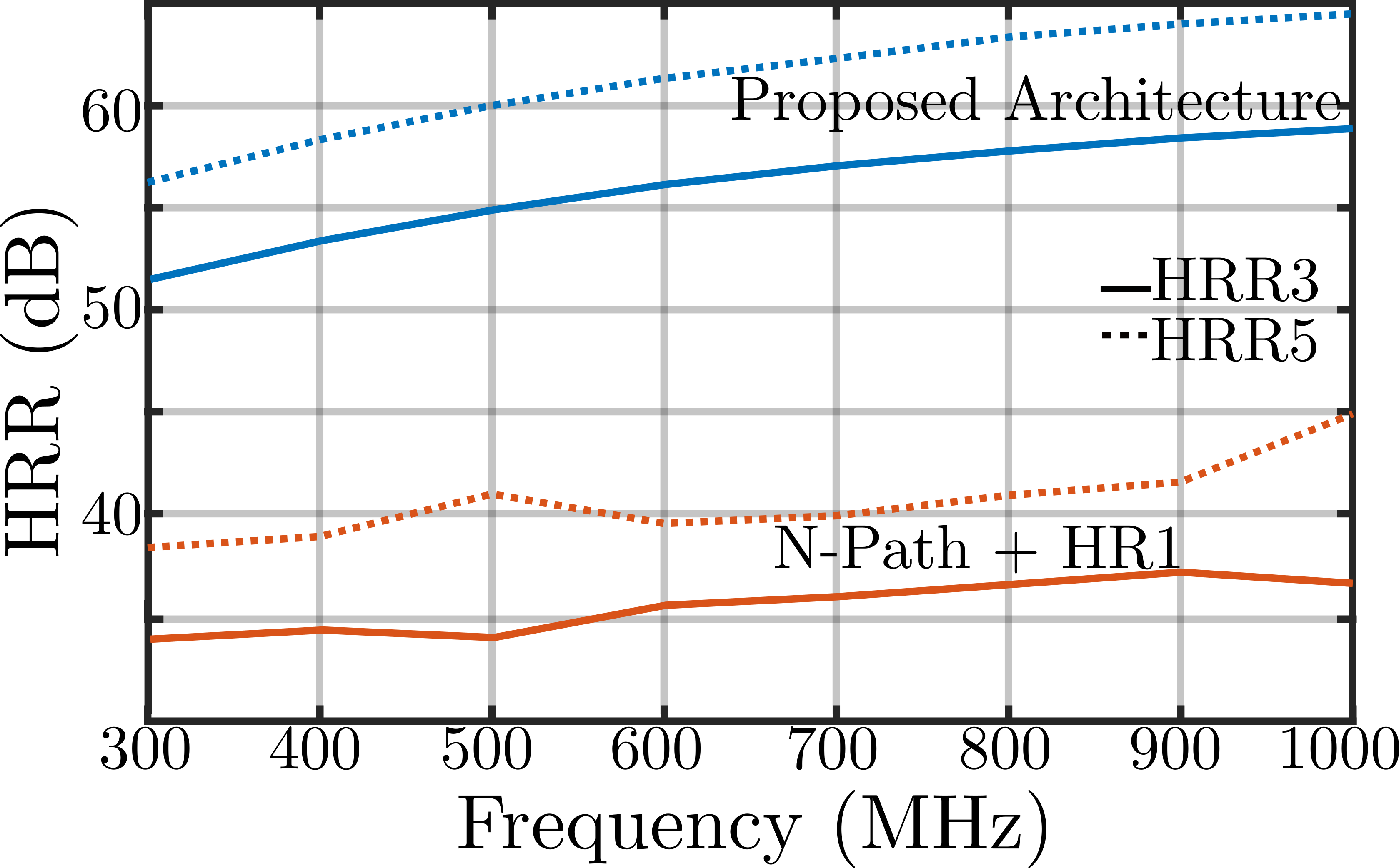
Harmonic rejection at the and the harmonics is shown in Fig. 8. The proposed architecture has effectively a second-order harmonic rejection at the and the harmonics, where as the combination of the N-path with HR1 has only first-order harmonic rejection. The second-order harmonic rejection is due to the suppression of the and the harmonics at the input of the N-path filter. A total harmonic rejection of approximately 50-60 dB is observed in the proposed architecture.
Simulated noise figure and S11 at MHz are 6.5 dB and -15 dB respectively. The 3-dB blocker compression point, B3dB, is simulated by observing the blocker level around and which reduces the small-signal gain at at the output of HR1 by 3dB. For the proposed architecture the B3dB resulting from the and the harmonics of is +2.1 dBm and +8.4 dBm respectively. The B3dB for N-path + HR1, without the feedback loop, is -6.5 dBm and -3.4 dBm respectively.
IV Conclusion
A harmonic suppressing N-path filter that employs a a harmonic selective combiner in the feedback path with a PWM-LO based upconverter is proposed. A baseband harmonic combiner is employed with the feedback loop at the output of the N-path filter, to select the desired signal from the input spectrum. The HRM in the feedback generates the and the harmonics responses, which effectively attenuates the harmonic responses observed at these frequencies at the input of the N-path filter. Due to this attenuation, the design operates as a second-order harmonic-rejection downconverter. Simulation results using commercial 65-nm CMOS devices are presented.
References
- [1] L. E. Franks and I. W. Sandberg, “An alternative approach to the realization of network transfer functions: the N-path filter,” Bell System Technical Journal, vol. 39, no. 5, pp. 1321–1350, Sep. 1960.
- [2] B. W. Cook, A. Berny, A. Molnar, S. Lanzisera, and K. S. J. Pister, “Low-power 2.4-GHz transceiver with passive RX front-end and 400-mV supply,” IEEE Journal of Solid-State Circuits, vol. 41, no. 12, pp. 2757–2766, Dec. 2006.
- [3] M. Darvishi, R. van der Zee, and B. Nauta, “Design of active N-path filters,” IEEE Journal of Solid-State Circuits, vol. 48, no. 12, pp. 2962–2976, Dec. 2013.
- [4] V. S. Rayudu, H. Kang, and R. Gharpurey, “An N-path filter with multiphase PWM clocks for harmonic response suppression,” in IEEE 11th Latin American Symposium on Circuits and Systems (LASCAS), Feb. 2020, pp. 1–4.
- [5] C. Andrews and A. C. Molnar, “A passive mixer-first receiver with digitally controlled and widely tunable RF interface,” IEEE Journal of Solid-State Circuits, vol. 45, no. 12, pp. 2696–2708, Dec. 2010.
- [6] D. Murphy, H. Darabi, and H. Xu, “A noise-cancelling receiver resilient to large harmonic blockers,” IEEE Journal of Solid-State Circuits, vol. 50, no. 6, pp. 1336–1350, Jun. 2015.
- [7] Y. Xu, J. Zhu, and P. R. Kinget, “A blocker-tolerant RF front end with harmonic-rejecting N-path filter,” IEEE Journal of Solid-State Circuits, vol. 53, no. 2, pp. 327–339, Feb. 2018.
- [8] X. He and H. Kundur, “A compact SAW-less multiband WCDMA/GPS receiver front-end with translational loop for input matching,” in IEEE International Solid-State Circuits Conference, Feb. 2011, pp. 372–374.
- [9] W.-G. Ho, T. Forbes, V. Singh, and R. Gharpurey, “An active interference cancellation technique with harmonic rejection for a broadband channelizer,” in IEEE 56th International Midwest Symposium on Circuits and Systems (MWSCAS), Aug. 2013, pp. 586–589.
- [10] A. Ghaffari, E. A. M. Klumperink, and B. Nauta, “A differential 4-path highly linear widely tunable on-chip band-pass filter,” in Proc. IEEE Radio Freq. Integr. Circuits (RFIC) Symp., May 2010, pp. 299–302.
- [11] H. Kang, W.-G. Ho, V. K. Singh, and R. Gharpurey, “A wideband receiver employing PWM-based harmonic rejection downconversion,” IEEE Journal of Solid-State Circuits, vol. 53, no. 5, pp. 1398–1410, May 2018.
- [12] K. Y. Kim and R. Gharpurey, “A 1.6 GS/s spectrum channelizer with PWM-LO based sub-band equalization,” in IEEE Custom Integrated Circuits Conference (CICC), Apr. 2021, pp. 1–2.
- [13] Z. Ru, N. A. Moseley, E. A. M. Klumperink, and B. Nauta, “Digitally enhanced software-defined radio receiver robust to out-of-band interference,” IEEE Journal of Solid-State Circuits, vol. 44, no. 12, pp. 3359–3375, Dec. 2009.
- [14] T. Forbes, W.-G. Ho, and R. Gharpurey, “Design and analysis of harmonic rejection mixers with programmable LO frequency,” IEEE Journal of Solid-State Circuits, vol. 48, no. 10, pp. 2363–2374, Oct. 2013.
- [15] S. Pavan and E. A. M. Klumperink, “Analysis of the effect of source capacitance and inductance on N-path mixers and filters,” IEEE Transactions on Circuits and Systems I: Regular Papers, vol. 65, no. 5, pp. 1469–1480, May 2018.
- [16] S. Manetti, “Passive switched capacitor filters: general biquad topology,” Electronics Letters, vol. 20, no. 2, p. 101, Jan. 1984.
- [17] J. Weldon, R. Narayanaswami, J. Rudell, L. Lin, M. Otsuka, S. Dedieu, L. Tee, K.-C. Tsai, C.-W. Lee, and P. Gray, “A 1.75-GHz highly integrated narrow-band CMOS transmitter with harmonic-rejection mixers,” IEEE Journal of Solid-State Circuits, vol. 36, no. 12, pp. 2003–2015, Dec. 2001.